
Professional PCB manufacturing and assembly
Building 6, Zone 3, Yuekang Road,Bao'an District, Shenzhen, China
+86-13410863085Mon.-Sat.08:00-20:00

Quality Inspection Standard for Double sided PCB and Multilayer PCB
In fact, many customers are not very clear about the quality inspection standards for double-sided circuit boards and multilayer circuit boards. Today, we will introduce the details of the IPC international inspection standards for circuit boards, so that we can correctly inspect the quality of PCB.
Scope: This standard is applicable to the inspection of base material, metal coating, solder resistance, characters, appearance, holes, warpage and other items of products. When this standard is not suitable for a certain manual manufacturing process or does not conform to the customer's requirements, the standard agreed with the customer shall prevail.
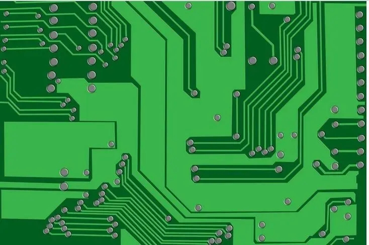
1、 Inspection requirements
1. Base (bottom) material:
1.1 Appearance of white spot reticulated fiber
White spot reticulation is acceptable if it meets the following requirements:
(1) Not more than 5% of the plate area
(2) The white spot in the line spacing shall not occupy 50% of the line spacing
1.2 Hierarchical blistering of halo is unacceptable
1.3 Foreign debris
Foreign matters of the base material are acceptable if they meet the following requirements:
(1) Identifiable as non-conductive material
(2) The wire spacing shall not be reduced by more than 50% of the original wire spacing
(3) The longest dimension is not more than 0.75mm
1.4 The base material shall not have copper foil layered and warped, and shall not have fiber hidden.
1.5 The base material model meets the specified requirements
2 Warpage tolerance (see the table below)
Plate thickness tolerance (mm) 0.2-1.2mm and above 1.5mm Double sided plate tolerance ≤ 1% ≤ 0.7% Multilayer plate tolerance ≤ 1% ≤ 0.7%
3. Plate thickness tolerance: the plate thickness meets the customer's requirements.
The maximum thickness tolerance of rigid finished double-sided multilayer plates is shown in the following table
Plate thickness mm Double sided plate tolerance mm Multilayer plate tolerance mm 0.2-1.0 ± 0.1 1.2-1.6 ± 0.13 ± 0.15 2.0-2.6 ± 0.18 ± 0.18 3.0 above ± 0.18 ± 0.2
Requirements for 4 holes:
4.1 The hole diameter meets the customer's requirements, and its tolerance range is as follows:
Aperture mmPTH Aperture tolerance mmNPTH Aperture tolerance less than 1.6mm ± 0.08 ± 0.05 greater than 1.6mm ± 0.1 ± 0.05
Note: The hole location shall meet the requirements of the drawing
4.2 It is not allowed to have multiple holes, fewer holes, holes not drilled through, plug holes, etc.
4.3 There shall be no deformed holes (such as round holes drilled into oval holes, trumpet holes, oval holes drilled into round holes, etc.).
4.4 The final hole diameter shall not be affected by copper slag, tin slag, etc.
4.5 The exposed copper on the inner wall of the component hole shall not exceed 3 points, and the total area shall not exceed 10% of the hole wall area, and the exposed copper shall not be annular.
4.6 The hole area in the hole shall not be greater than 0.5mm, and the number of each hole shall not exceed 2 points. Such holes shall not exceed 5% of the total number of holes. It is not allowed to have annular cavities in the holes and hole corners broken or without copper. All metallized holes on the multilayer board that are connected to the inner layer with electrical appliances should not have holes.
4.7 No conducting hole is allowed.
4.8 Coating wrinkles in holes shall meet the following requirements:
(1) It will not cause poor connection of the inner layer.
(2) Meet the coating thickness requirements.
(3) The combination with the hole wall is good.
5 Pads
5.1 The bonding pad shall be at least 0.1mm, and the ring width of the part connected with the line shall be reduced by not less than 50% of the line width due to misalignment,
5.2 The area of the pad reduced due to pinholes and notches shall not exceed 1/5 of the pad.
5.3 Three pinholes within 0.05mm2 are allowed at the SMD position.
5.4 The pads on the solder resist are as follows (as shown in the figure):
(1) The total area of the pad on any two or three sides shall not exceed 10% of the pad.
(2) The pad on one side shall not exceed 5% of the pad area.
Note: The shaded part is solder resist
6 Lines
6.1 No short circuit or open circuit is allowed
6.2 The line gap is allowed to exist, but it shall be ensured that the line gap will not reduce the line by more than 20% of the design line width. When the line width is greater than 3mm, the width of the line gap or line hole is less than 1/3 of the line, and the length of the hole or gap does not exceed the wire width, it is acceptable, but this situation cannot exceed two places on the same board.
Note: notch ---- exposing the substrate at the concave point at the edge of the line
6.3 The ratio of the maximum diameter of needle holes and sand holes to the line width shall be less than 1/5, and there shall be no more than three places on the same line.
6.4 The wire width tolerance shall not exceed ± 20% of the original design line width, and the line spacing tolerance shall not exceed ± 20% of the original design value.
6.5 The single point projection or depression of the line shall not exceed ± 20% of the original design line width.
6.6 The metal residue on each circuit board shall not exceed three points, and the line width or line spacing shall not be increased or decreased by more than 30% of the original design value.
6.7 Sawtooth shape is not allowed for line width.
6.8 No twisted lines are allowed.
7 Solder resistance film (green oil)
7.1 The model, color and brand of the ink used must be consistent with the ink specified by the customer. If the customer does not specify, the company's requirements shall apply.
7.2 If required by the customer, the upper and lower limits of the sample plate shall be taken as the scope of delivery.
7.3 During normal soldering, the solder mask shall not bubble and the paint surface shall not fall off.
7.4 The printing of solder mask must be uniform on the whole surface and have the same color.
7.5 The repair of solder mask shall not exceed three points on the same surface (the fingerboard surface is more than 100mm2), and the length of each point shall not exceed 5mm. After repair, it shall be smooth and uniform in color.
7.6 Apply 3M600 # adhesive tape to the board surface. After 30 seconds, pull it up at an angle of 900 with the board surface. No green oil shall fall off.
7.7 The area of the pad on the solder mask of the solder joint of the part foot shall not be 900 arcs intersecting the outer ring of the pad,
8.1 The copper foil under the solder mask shall be free from oxidation, stains, line burning, etc.
8.2 No flux blocking agent is allowed to enter the part hole (the non part through hole shall be sealed according to the customer's needs).
8.3 It is not allowed to cross two lines with foreign matters such as fluff in resistance welding, and it is allowed to have non conductive objects such as fluff with a length of less than 1mm, but not more than 2 per square inch.
8.4 The thickness of resistance welding on the line shall not be less than 10um.
8.5 The waves or lines on the resistance welding surface have not affected the upper and lower limits of the specified thickness, and the wires have slightly wrinkled, but have not caused void, and the adhesion is good.
8.2 Metal coating and tin coating
9.1 The metal coating shall be free from poor electroplating phenomena such as roughness and finger prints.
9.2 Metal coating shall be tested with 3M600 # tape, and there shall be no coating peeling or blistering delamination.
9.3 The thickness of the coating on the sunken part of the line shall not be less than 15 um, and the sunken area shall not exceed 4 mm, with no more than two points on each plate.
9.4 Coating and tin spraying thickness of tin spraying plate
(1) The coating thickness shall be greater than 3 um, and the thickest shall not cause small holes.
(2) The average value of the hole and the coating thickness shall not be less than 25 um, the minimum value shall not be less than 20 um, and the maximum value shall not cause the hole to be small.
(3) The tin spraying layer is smooth and bright, and the lead tin alloy surface is free of pollution and discoloration.
9.5 Plating thickness of gold plate
The minimum thickness of copper plating in the hole shall not be less than 10 um, the thickness of nickel coating on the line shall not be less than 5 um, and the average thickness of nickel coating in the hole shall not be less than 5 um. The appearance of the gold plating layer is uniform and golden, with no oxidation, pollution and discoloration.
9.6 Metal particles in the line part within the formed line can be allowed to exist, but the total area shall not be greater than 3mm2, and shall not be greater than 50% of the distance between the plate edge and the line.
9.7 It is not allowed to scratch the line and expose the base material. The same side of the line that is scratched and does not expose the base material shall not exceed 2, and the length shall not exceed 5 mm, but the scratch depth shall not exceed 3 um.
9.8 Resistance welding scratch shall not lead to exposed metal layer. If the scratch width does not exceed 0.05mm and the length does not exceed 5mm, two pieces are allowed on the same plate.
9.9 No more than 3 open circuit patching lines shall be used for double sided boards, and they shall not be on the same surface. Only 2 patching lines are allowed for multilayer boards, and the patching line length shall not exceed 3mm. The patching line position shall be 1mm away from the bonding pad, and the corner shall not be patched.
9.10 The line shall not be stained with tin.
9.11 There shall be no obvious milling chips in the contour processing. The edge of the milling processing plate shall be smooth, the punching contour shall be neat, the plate edge shall be free of bursting defects, and the plate surface shall be free of ink residues, corrosive residues, oil stains, glue stains, finger prints, sweat stains and other pollutants.
10 Golden Finger
10.1 The thickness of the nickel layer of the gold finger shall not be less than 5um. When the customer requires gold plating but does not specify the coating thickness, the gold thickness shall not be less than 0.5 um. When the customer requires gold plating but does not specify the thickness, the gold thickness shall not be less than 0.05 um.
10.3 The gold finger shall be free from oxidation, burning, pollution and glue stains, and there shall be no residual copper or other foreign matters within the distance. The color shall be gold.
10.4 The edge of gold finger shall not be warped or damaged.
10.5 The length of notch at the edge of gold finger shall not be greater than 0.15mm2, and only one piece of gold finger is allowed to exist on each piece of gold finger. Such gold finger shall not exceed two pieces on each plate.
10.6 Stick 3M600 # adhesive tape on the gold finger. After 30 seconds, pull it up at an angle of 900 with the board surface. No gold or nickel shall fall off or rise (i.e., throw gold or nickel)
10.7 Two scratches with a length of 2mm and a depth of less than 3um are allowed in the gold finger, but copper and nickel shall not be exposed. The scratches shall not be located at 3/5 of the middle of the gold finger. Such gold fingers shall not be more than two on the same plate.
10.8 The number of gold fingers with pinholes, dents, indentations and cavities is less than 2 (including 2), but the notch length is within 0.15 um, and nickel and copper are not exposed. The number of gold fingers with defects on each plate cannot exceed 2, but the defects cannot be located at 3/5 of the middle part of the gold finger.
10.9 The solder mask is allowed to cover the edge of the gold finger with a maximum of 1.5mm (when the use of the gold finger is not affected).
11 Text symbol
3.11.1 Check whether the characters are single or double sided according to the customer's requirements.
11.2 The color, model and brand of character ink shall meet the customer's requirements.
11.3 The coincidence and integrity of characters shall be clear and uniform.
11.4 Characters are generally not allowed to enter the upper pad or SMD position (unless allowed by the customer's master drawing).
10.1 Check whether the customer requires to add marks and cycles in the text process, and whether the added positions meet the customer's requirements.
10.2 The polarity symbol, part symbol and pattern cannot be wrong.
10.3 Characters shall not have double images or be illegible, or be misunderstood due to incompleteness (such as P, R, D, B).
10.4 Use 3M600 # adhesive tape to stick it on the surface of characters. After 30 seconds, pull it with a force perpendicular to the surface of the plate, and no characters shall fall off.
11 Marking
11.1 When the customer needs the following marks or some of them, they should be printed on the specified level and position: the company's marks, customer marks, UL marks, manufacturing date, customer part number (P/N), material and flammability marks.
11.2 The marked layers (such as lines, solder mask, characters, inner layers, etc.) are correct, and the marks are complete and clear; Incomplete parts shall not lead to misreading and misrecognition.
12 Overall dimensions and machining
12.1 The overall dimension tolerance of the plate is as follows
Milling edge ± 0.15mm ± 0.2mm
Punch plate ± 0.15mm ± 0.15mm
12.2 The overall dimension tolerance of the special-shaped hole is ± 0.1mm, and the distance tolerance between the center of the special-shaped hole and the edge shall be less than ± 0.15mm.
12.3 Plate edge: the plate edge or special-shaped hole and groove milled by CNC shall be smooth without copper exposure; The punched edges or special-shaped holes and grooves shall be free of explosion, defect and damage to the circuit, and the edges shall be neat.
12.4 Machining shall be subject to the customer's requirements when the customer has tolerance requirements.
12.5 The angle and length of the beveled plate shall meet the customer's requirements, and the surface of the beveled edge shall be smooth, uniform, neat and consistent.
12.6 After V-CUT, the appearance of single plate shall meet the specified requirements, and the V-CUT depth shall be uniform.
The remaining plate thickness tolerance after V-cut is shown in the following table:
Plate thickness (mm) above 0.81.01.21.62.02.5
V-CUT residual thickness (mm) 0.2-0.30.2-0.30.3-0.40.4-0.50.5-0.60.5-0.7
When the plate thickness is less than 0.8mm, it shall be separately agreed with the customer, and the V-CUT shall not have copper exposure. The V-CUT line shall be straight and the width shall meet the specified requirements.
13 Physical properties 3.13.1 Solderability:
(1) The tin temperature is 245 ± 50C, the neutral flux and the test sample are wetted within 3 ± 1s, and the non weldable part of the gold plate cannot exceed 5%, and cannot be concentrated in the same area; The tin plate shall be fully wetted.
(2) After the solderability test, the solder mask characters shall not bubble or fall off.
(3) There shall be no blowing hole, explosion hole or separation from the hole wall.
(4) The warpage of the plate shall meet the specified requirements.
(5) There is no delamination of the substrate.
13.2 Thermal shock
Conditions: Dip tin for three times at a tin temperature of 288 ± 0C for 10 seconds each time. Cool to room temperature after each dip. The following conditions shall not occur after three times of tin dipping:
(1) The base material shall not be layered, and the copper foil shall not be bubbled or warped.
(2) There shall be no layering in the inner layer of the multilayer board.
(3) The coating in the hole shall be free of fracture or delamination.
(4) Do not blow or burst holes.
13.3 Solvent resistance test of resistance welding characters
After the solvent resistance test of solder mask characters by the method specified by the company, there shall be no peeling, dissolution, swelling, rough surface and obvious discoloration.
13.4 Slicing
After the method test specified by the company is completed, the observed and measured conditions shall be:
(1) The coating thickness in the hole shall meet the specified requirements.
(2) The coating in the hole is well combined with the hole wall without cracks.
(3) The coating in the hole of the multilayer board is well bonded with the inner copper layer without cracks.
(4) The hole is intact.
(5) The coating in the hole shall be uniform, the thickness error in the hole shall not exceed ± 30%, and the average value shall meet the specified requirements.

Detailed explanation of PCB process PCB layers
Oct 30,2022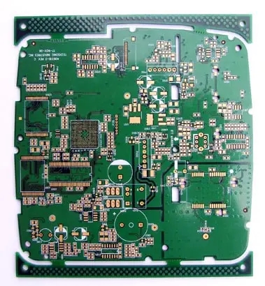


Just upload Gerber files, BOM files and design files, and the KINGFORD team will provide a complete quotation within 24h.