
Professional PCB manufacturing and assembly
Building 6, Zone 3, Yuekang Road,Bao'an District, Shenzhen, China
+86-13410863085Mon.-Sat.08:00-20:00

In order to suppress EMI, the EMI design of digital circuit shall follow the following principles:
According to the relevant EMC/EMI technical specifications, the indicators are decomposed into single board circuits for hierarchical control.
The three elements of EMI, namely interference source, energy coupling path and sensitive system, are controlled to make the circuit have a flat frequency response and ensure the normal and stable operation of the circuit.
Start with the front-end design of the equipment, pay attention to the EMC/EMI design, and reduce the design cost.
2 EMI Control Technology of Digital Circuit PCB
When dealing with various forms of EMI, specific problems must be analyzed. In PCB design of digital circuit, EMI control can be carried out from the following aspects.
2.1 Device selection
In EMI design, the speed of selected devices should be considered first. For any circuit, if a device with a rise time of 5 ns is replaced by a device with a rise time of 2.5 ns, the EMI will be increased by about 4 times. The radiation intensity of EMI is proportional to the square of the frequency. The highest EMI frequency (fknee) is also called EMI transmission bandwidth, which is a function of signal rise time rather than signal frequency:
Fknit=0.35/Tr (where Tr is the signal rise time of PCB device)
The frequency range of this radiated EMI is 30MHz to several GHz. In this frequency band, the wavelength is very short, and even very short wiring on the circuit board may become a transmitting antenna. When EMI is high, the circuit is easy to lose its normal function. Therefore, in terms of device selection, on the premise of ensuring circuit performance requirements, low-speed chips should be used as far as possible and appropriate drive/receive circuits should be used. In addition, because the lead pins of devices have parasitic inductors and capacitors, the impact of device packaging on signals cannot be ignored in high-speed design, because it is also an important factor to generate EMI radiation. Generally, the parasitic parameters of SMD are less than those of plug-in devices, and the parasitic parameters of BGA package are less than those of QFP package.
2.2 Selection of connectors and definition of signal terminals
The connector is the key link of high-speed signal transmission, and also the weak link prone to EMI. In the terminal design of the connector, more ground pins can be arranged to reduce the distance between the signal and the ground, reduce the effective signal loop area that generates radiation in the connector, and provide a low impedance return path. If necessary, consider isolating some key signals with ground pins.
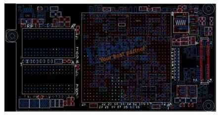
2.3 Stack design
On the premise of cost permitting, increasing the number of ground wire layers and placing the signal layer close to the ground plane layer can reduce EMI radiation. For high-speed PCB, the power layer and ground layer are closely coupled, which can reduce the power impedance and thus reduce EMI.
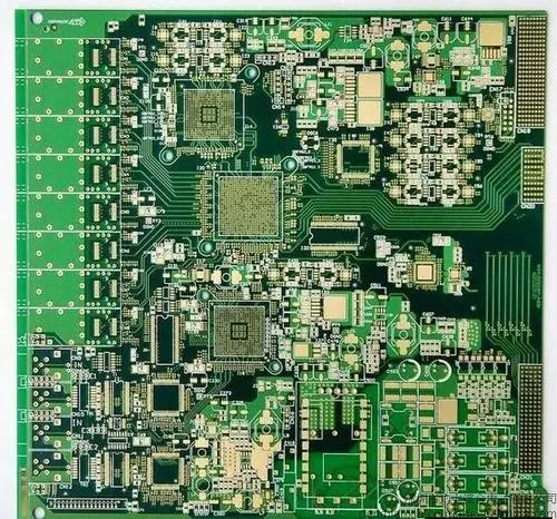
2.4 PCB layout
According to the flow direction of signal current, reasonable layout can reduce the interference between signals. Rational layout is the key to controlling EMI. The basic principles of layout are:
Analog signal is easily interfered by digital signal, and analog circuit shall be separated from digital circuit;
The clock line is the main interference and radiation source, which shall be far away from the sensitive circuit, and the clock line shall be the shortest;
High current and high power consumption circuits shall not be arranged in the central area of the board as far as possible, and the effects of heat dissipation and radiation shall be considered at the same time;
The connector shall be arranged at one side of the board as far as possible and away from the high-frequency circuit;
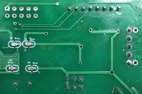
The input/output circuit is close to the corresponding connector, and the decoupling capacitor is close to the corresponding power supply pin;
Fully consider the feasibility of layout on power division. Multi power devices should be placed across the boundary of power division area to effectively reduce the impact of plane division on EMI;
The return plane (path) is not divided.
2.5 PCB wiring
Impedance control: high-speed signal lines will show the characteristics of transmission lines. Impedance control is required to avoid reflection, overshoot and ringing of signals and reduce EMI radiation.
Strictly control the routing length, number of vias, cross partition, termination, wiring layer, return path, etc. of clock signals (especially high-speed clock signals).
The signal loop, that is, the loop formed by the signal flowing out to the signal flowing in, is the key to EMI control in PCB design and must be controlled during wiring. To understand the flow of each key signal, the key signal shall be routed close to the return path to ensure the minimum loop area.
EMI Control Technology in Digital Circuit PCB Design
For low-frequency signals, the current shall flow through the path with the minimum resistance; For high-frequency signals, the high-frequency current should flow through the path with the smallest inductance, rather than the path with the smallest resistance. For differential mode radiation, the EMI radiation intensity (E) is proportional to the current, the area of the current loop, and the square of the frequency. (Where I is the current, A is the area of the loop, f is the frequency, r is the distance to the center of the loop, and k is a constant.)
Therefore, when the minimum inductance return path is just below the signal conductor, the current loop area can be reduced, thus reducing the EMI radiation energy.
3Other EMI control means
3.1 Power system design
The low impedance power supply system is designed to ensure that the impedance of the power distribution system in the frequency range lower than fknee is lower than the target impedance.
Use filters to control conducted interference.
Decoupling of power supply. In EMI design, reasonable decoupling capacitor can make the chip work reliably, reduce high-frequency noise in the power supply, and reduce EMI. Due to the influence of PCB wire inductance and other parasitic parameters, the response speed of power supply and its supply wire is slow, which will make the instantaneous current required by the driver in high-speed circuit insufficient. By properly designing the bypass or decoupling capacitor and the distributed capacitor of the power supply layer, the energy storage function of the capacitor can be used to quickly provide current for the device before the power supply responds. Proper capacitive decoupling can provide a low impedance power supply path, which is the key to reduce common mode EMI.
3.2 Grounding
The grounding design is the key to reduce the EMI of the whole board.
Single point grounding, multi-point grounding or mixed grounding shall be adopted.
Digital ground, analog ground and noise ground shall be separated, and a suitable public grounding point shall be determined
If there is no ground wire layer in the double panel design, it is important to reasonably design the ground wire grid, and ensure the width of ground wire>width of power wire>width of signal wire. It is also possible to use large-area floor covering, but it should be noted that large-area land on the same layer has good consistency.
For the design of multilayer PCB board, the ground plane layer shall be ensured to reduce the common ground impedance.
3.3 Series damping resistance
On the premise that the circuit timing requirements allow, the basic technology for suppressing interference sources is to connect a small resistance value resistor in series at the key signal output terminal, usually 22~33 Ω. These small resistors connected in series at the output terminals can slow down the rise/fall time and make the overshoot and undershoot signals smoother, thus reducing the high-frequency harmonic amplitude of the output waveform and effectively restraining EMI.


Just upload Gerber files, BOM files and design files, and the KINGFORD team will provide a complete quotation within 24h.