
Professional PCB manufacturing and assembly
Building 6, Zone 3, Yuekang Road,Bao'an District, Shenzhen, China
+86-13410863085Mon.-Sat.08:00-20:00


PCB Design Objective of DC Motor Drive Circuit
In the design of DC motor drive circuit, the following points are mainly considered:
1. Function: Does the motor rotate in one direction or two directions? Need speed regulation? For unidirectional motor drive, just use a high-power triode or FET or relay to directly drive the motor. When the motor needs to rotate in both directions, use the H-bridge circuit composed of four power PCB components or use a double pole double throw relay. If speed regulation is not required, just use the relay; However, if speed regulation is required, switching elements such as triode and FET can be used to realize PWM (pulse width modulation) speed regulation.
2. Performance: For the motor drive circuit with PWM speed regulation, the following performance indicators are mainly available.
1) Output current and voltage range, which determines how much power the circuit can drive the motor.
2) Efficiency, high efficiency means not only saving power, but also reducing the heating of the drive circuit. To improve the efficiency of the circuit, we can start with ensuring the switching state of power devices and preventing common state conduction (a problem that may occur in the H-bridge or push-pull circuit is that two power devices are conducted simultaneously to short circuit the power supply).
3) Influence on control input. The power circuit shall have good signal isolation for its input terminal to prevent high voltage and large current from entering the main control circuit, which can be isolated with high input impedance or optocoupler
4) Impact on power supply. Common state conduction can cause the instantaneous drop of power supply voltage and cause high-frequency power pollution; Large currents may cause ground wire potential to float.
5) Reliability. The motor drive circuit shall be as safe as possible, no matter what control signal and passive load are added.
1. Input and level conversion:
The input signal line is led in by DATA, pin 1 is the ground wire, and the rest is the signal line. Note that pin 1 is connected to the ground with a 2K ohm resistance. When the drive board and the microcontroller are powered separately, this resistor can provide a path for signal current return. When the driver board shares a set of power supplies with the microcontroller, this resistance can prevent the high current from flowing along the line to the ground wire of the microcontroller motherboard to cause interference. In other words, it is equivalent to separating the ground wire of the drive board from the ground wire of the microcontroller to achieve "one point grounding".
The high-speed operational amplifier KF347 (TL084 can also be used) is a comparator, which compares the input logic signal with the 2.7V reference voltage from the indicator lamp and a diode, and converts it into a square wave signal close to the power supply voltage amplitude. The input voltage range of KF347 cannot be close to the negative supply voltage, otherwise an error will occur. Therefore, a diode is added at the input end of the operational amplifier to prevent the voltage range from overflowing. One of the two resistors at the input is used to limit the current, and the other is used to pull the input to the low level when the input is suspended.
The LM339 or any other open circuit output comparator cannot be used to replace the op amp, because the output impedance of the high level state of the open circuit output is more than 1 kiloohm, the voltage drop is large, and the later stage of the triode cannot be cut off.
2. Grid drive part:
The circuit composed of the rear triode, resistor and voltage stabilizing tube further amplifies the signal, drives the gate of the FET, and uses the gate capacitor of the FET itself (about 1000pF) for delay to prevent the simultaneous conduction ("common state conduction") of the FETs on the upper and lower arms of the H bridge from causing a power short circuit.
When the output terminal of the operational amplifier is at low level (about 1V to 2V, which cannot reach zero completely), the following triode is turned off and the FET is turned on. The upper triode is on, the FET is off, and the output is high. When the output terminal of the operational amplifier is at a high level (about VCC - (1V to 2V), which cannot fully reach VCC), the following triode is turned on and the FET is turned off. The upper triode is off, the FET is on, and the output is low level.
The above analysis is static, and the dynamic process of switching is discussed below: the on resistance of the triode is far less than 2 kiloohms, so when the triode is switched from off to on, the charge on the grid capacitor of the FET can be released quickly, and the FET can be switched off quickly. However, when the triode is switched from on to off, it takes some time for the MOSFET grid to charge through a 2 kiloohm resistor. Accordingly, the conversion speed of FET from on to off is faster than that from off to on. If the switching action of two triodes occurs at the same time, this circuit can make the upper and lower arms of the FET switch off first and then on, eliminating the common state conduction phenomenon.
In fact, it takes a certain time for the output voltage of the operational amplifier to change. During this time, the output voltage of the operational amplifier is in the middle of the positive and negative power supply voltages. At this time, the two triodes are turned on at the same time, and the FET is turned off at the same time. So the actual circuit is safer than this ideal situation.
The 12V zener diode of the FET grid is used to prevent the FET grid from overvoltage breakdown. The withstand voltage of the common FET grid is 18V or 20V, which will be broken down if the 24V voltage is added directly. Therefore, the voltage stabilizing diode cannot be replaced by a common diode, but it can be replaced by a resistance of 2k Ω, which can also obtain 12V voltage division.
3. FET output part:
There are diodes in reverse parallel between the source and drain inside the high-power FET. When connected to the H-bridge, it is equivalent to that the output terminal has four diodes in parallel for eliminating voltage spikes, so there is no external diode. Parallel connection of a small capacitor (between out1 and out2) at the output terminal has certain advantages in reducing the peak voltage generated by the motor, but it has the side effect of generating peak current when using PWM, so the capacity should not be too large. This capacitance can be omitted when using small power motors. If you add this capacitor, you must use a high withstand voltage capacitor. Ordinary ceramic chip capacitors may have breakdown and short circuit faults.
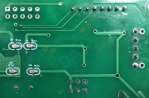
The circuit composed of resistor, LED and capacitor in parallel at the output terminal indicates the rotation direction of the motor
4. Performance index:
The power supply voltage is 15~30V, the maximum continuous output current is 5A/each motor, which can reach 10A in a short time (10 seconds), and the maximum PWM frequency can be 30KHz (generally 1~10KHz). The circuit board contains four logically independent power amplification units, whose output terminals are connected in pairs to form an H-bridge, which can be directly controlled by a single chip microcomputer. Realize bidirectional rotation and speed regulation of motor.
5. PCB layout and wiring for outsourcing proxy painting of PCB design:
The high current circuit should be as short and thick as possible, and avoid passing through the via as much as possible. If it must pass through the via, make the via larger (>1mm) and make a circle of small via on the bonding pad, and fill it with solder during welding, otherwise it may burn off. In addition, if a voltage stabilizing tube is used, the conductor from the source pole of the FET to the power supply and ground should be as short and thick as possible, otherwise, when the current is high, the voltage drop on this section of conductor may be burnt by the positive bias voltage stabilizing tube and the conducting triode. At the beginning of the design, a 0.15 ohm resistance was connected between the source pole and the ground of the NMOS transistor to detect the current, which became the culprit of the constant burning boards. Of course, this problem does not exist if the regulator tube is replaced by a resistor.
The PCB of motor drive circuit needs to adopt special cooling technology to solve the problem of power consumption. Printed circuit board (PCB) substrate (such as FR-4 epoxy glass) has poor thermal conductivity. On the contrary, copper has excellent thermal conductivity. Therefore, from the perspective of thermal management, increasing the copper area in PCB is an ideal solution. Thick copper foil (e.g., 2 ounces (68 microns thick)) has better thermal conductivity than thinner copper foil. However, the use of thick copper foil is costly and difficult to achieve fine geometry. As a result, it is common to use 1 oz (34 microns) of copper foil. Outer layer is usually used ½ Ounces to 1 ounce of copper foil. The solid copper surface used in the inner layer of multilayer circuit board has good heat dissipation. However, since these copper surfaces are usually placed in the center of the circuit board stack, the heat will accumulate inside the circuit board. Increase the copper area of the outer layer of PCB and connect or "seam" it to the inner layer through many through holes, which helps transfer heat to the outside of the inner layer.
Due to the existence of wiring and components, the heat dissipation of double-layer PCB may be more difficult. Therefore, it is necessary to provide as many solid copper surfaces as possible and achieve good thermal connection with motor driver ICs. Copper clad area is added on both outer layers and connected with many through holes to help heat dissipation between areas separated by wiring and components.
a. Wiring width: the wider the better
Since the input and output current of motor driver IC is large (more than 10A in some cases), the PCB wiring width of input and output devices should be carefully considered. The wider the wiring, the lower the resistance. The size of the wiring must be adjusted so that the wiring resistance does not consume too much power to avoid heating the wiring. Too small wiring can actually be used as an electric fuse, and it is easy to burn out!
Designers usually use IPC-2221 to determine the appropriate routing width. This specification provides corresponding charts showing copper cross-sectional area for various current levels and allowable temperature rise, which can be converted to the wire width under the condition of given copper layer thickness. For example, the wire carrying 10A current in an ounce copper layer needs to be slightly wider than 7mm to achieve a temperature rise of 10 ℃. For 1-A current, the wiring width only needs to be 0.3mm. In view of this, 10A current seems impossible to pass through the micro IC board.
Advantages of SMT surface mounting technology
Oct 27,2022


Just upload Gerber files, BOM files and design files, and the KINGFORD team will provide a complete quotation within 24h.