
Professional PCB manufacturing and assembly
Building 6, Zone 3, Yuekang Road,Bao'an District, Shenzhen, China
+86-13410863085Mon.-Sat.08:00-20:00

The domestic enterprises that can mass produce high-level circuit boardsmainly come from foreign-funded enterprises or a few domestic enterprises. The production of high-level circuit boards requires not only higher investment in technology and equipment, but also the accumulation of experience of technicians and production personnel. At the same time, the introduction of high-level board customer certification procedures is strict and cumbersome, so the threshold for high-level circuit boards to enter enterprises is high, and the industrialization production cycle is long.
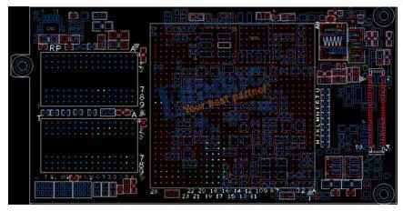
The average number of PCB layers has become an important technical indicator to measure the technical level and product structure of PCB enterprises. This paper briefly introduces the main processing difficulties encountered in, and introduces the control points of key production processes of high-level circuit boards for reference.
1、 Main production difficulties
Compared with the characteristics of conventional circuit boards, high layer circuit boards have the characteristics of thicker boards, more layers, denser lines and vias, larger unit sizes, thinner dielectric layers, etc. The requirements for inner layer space, inter layer alignment, impedance control and reliability are stricter.
1.1 Difficulties in interlayer alignment
Due to the large number of layers of high layer boards, the alignment requirements of the customer design end on each layer of PCB are becoming more and more strict. Generally, the alignment tolerance between layers is controlled by ± 75 μ m. Considering such factors as large unit size design of high-rise boards, ambient temperature and humidity of graphic transfer workshop, dislocation superposition and interlayer positioning mode caused by inconsistency of different core board layers, it is more difficult to control the interlayer alignment of high-rise boards.
1.2 Difficulties in making inner line
High TG, high speed, high frequency, thick copper, thin dielectric layer and other special materials are used for the high layer board, which puts forward high requirements for the inner layer circuit fabrication and graphic size control, such as the integrity of impedance signal transmission, which increases the difficulty of inner layer circuit fabrication. The line width and line spacing are small, the number of open and short circuits is increased, the number of short circuits is increased, and the qualification rate is low; There are many fine line signal layers, and the probability of AOI missing detection in the inner layer is increased; The inner core plate is thin, easy to fold, resulting in poor exposure, and easy to roll when etched; Most of the high-rise boards are system boards with large unit size, and the cost of scrapping finished products is relatively high.
1.3 Difficulties in pressing and manufacturing
Multiple inner layer core PCBs and semi solidified sheets are overlapped, and defects such as sliding plate, delamination, resin cavity and bubble residue are easy to occur during pressing production. When designing the laminated structure, it is necessary to fully consider the heat resistance, voltage resistance, glue filling amount and dielectric thickness of the material, and set a reasonable pressing program for the high-rise board. The number of layers is large, and the control of expansion and contraction and the compensation of size coefficient cannot keep consistent; The interlayer insulation layer is thin, which easily leads to the failure of interlayer reliability test. Figure 1 shows the defect diagram of cracked plate delamination after thermal stress test.
1.4 Difficulties in drilling
The use of high TG, high speed, high frequency, thick copper special plates increases the difficulty of drilling roughness, drilling burr and drilling dirt removal. The number of layers is large, the total copper thickness and plate thickness are accumulated, and the drilling tool is easy to break; CAF failure caused by many dense BGAs and narrow hole wall spacing; Inclined drilling is easy to occur due to the thickness of the plate.
2、 Key production process control
2.1 Material selection
With the development of high performance and multi-function of electronic components, high frequency and high-speed signal transmission is also brought. Therefore, low dielectric constant and dielectric loss of electronic circuit materials, low CTE, low water absorption and better high-performance copper clad laminate materials are required to meet the processing and reliability requirements of high layer boards. Commonly used PCB suppliers mainly include A series, B series, C series and D series. The main characteristics of these four inner substrates are compared.
For the high layer thick copper circuit board, the prepreg with high resin content is selected. The glue flow of the interlayer prepreg is enough to fill the inner layer graphics. If the insulating medium layer is too thick, the finished board is prone to be super thick. Otherwise, if the insulating medium layer is too thin, it is easy to cause quality problems such as dielectric layering, high-voltage test failure, etc. Therefore, the selection of insulating medium materials is extremely important.
2.2 Structural design of laminated layer
The main factors considered in the design of the laminated structure are the heat resistance, voltage resistance, glue filling amount and dielectric layer thickness of the material, which should follow the following main principles.
(1) The prepreg and core board manufacturers must be consistent. To ensure the reliability of PCB, single 1080 or 106 prepreg shall not be used for all layers of prepreg (unless the customer has special requirements). If the customer has no requirements for media thickness, the thickness of media between layers must be ≥ 0.09mm according to IPC-A-600G.
(2) When customers require high TG plates, core plates and prepreg shall be made of corresponding high TG materials.
(3) The inner substrate is 3OZ or above, and the semi solidified sheet with high resin content is selected, such as 1080R/C65%, 1080HR/C 68%, 106R/C 73%, 106HR/C76%; However, the structural design of 106 high glue semi curing sheet shall be avoided as far as possible to prevent multiple 106 semi curing sheets from overlapping. Because the glass fiber yarn is too thin, it will collapse in the large base material area, which will affect the dimensional stability and delamination.
(4) If the customer has no special requirements, the thickness tolerance of the interlayer medium layer is generally controlled by+/- 10%. For the impedance plate, the thickness tolerance of the medium is controlled by IPC-4101 C/M level tolerance. If the impedance influencing factors are related to the thickness of the base material, the tolerance of the plate must also be controlled by IPC-4101 C/M level tolerance.
2.3 Interlayer alignment control
For the accuracy of the size compensation of the inner core plate and the control of the production size, it is necessary to accurately compensate the graphic size of each layer of the high-rise board through the data and historical data experience collected in the production for a certain period of time to ensure the consistency of the rise and fall of each layer of the core plate. Select high-precision and reliable interlayer positioning mode before pressing, such as four groove positioning (Pin LAM), hot melt and rivet combination.
Setting appropriate pressing process procedures and daily maintenance of the press is the key to ensure the pressing quality, control the glue flow and cooling effect, and reduce the interlayer dislocation. The inter layer alignment control needs to be comprehensively considered from the inner layer compensation value, pressing positioning mode, pressing process parameters, material characteristics and other factors.
2.4 Inner PCB circuit process
Because the analytical ability of traditional exposure machine is 50 μ About m, for the production and manufacture of high-rise boards, the laser direct imaging machine (LDI) can be introduced to improve the graphic analysis ability, which reaches 20 μ M or so. The alignment accuracy of traditional exposure machine is ± 25 μ m. The inter storey alignment accuracy is greater than 50 μ m。 Using high-precision alignment exposure machine, the graphic alignment accuracy can be increased to 15 μ M, and the inter floor alignment accuracy is controlled by 30 μ Within m, the alignment deviation of traditional equipment is reduced, and the inter storey alignment accuracy of high-rise slabs is improved.
In order to improve the etching capacity of the circuit, it is necessary to give appropriate compensation to the width of the circuit and PCB pad (or solder ring) in the engineering design, as well as more detailed design consideration to the compensation amount of special graphics, such as return lines, independent lines, etc. Confirm whether the design compensation for inner layer line width, line distance, isolation ring size, independent line, hole to line distance is reasonable, or change the engineering design.
With PCB impedance and inductive reactance design requirements, pay attention to whether the design compensation of independent lines and PCB impedance lines is sufficient. Control the parameters during etching. Batch production can only be carried out after the first article is confirmed to be qualified. In order to reduce side etching, it is necessary to control the composition of each liquid medicine in the etching solution within the optimal range. The traditional etching line equipment has insufficient etching capacity. The equipment can be technically modified or high-precision etching line equipment can be imported to improve the uniformity of etching and reduce the problems such as rough edges and unclean etching.


Just upload Gerber files, BOM files and design files, and the KINGFORD team will provide a complete quotation within 24h.