
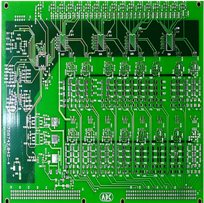
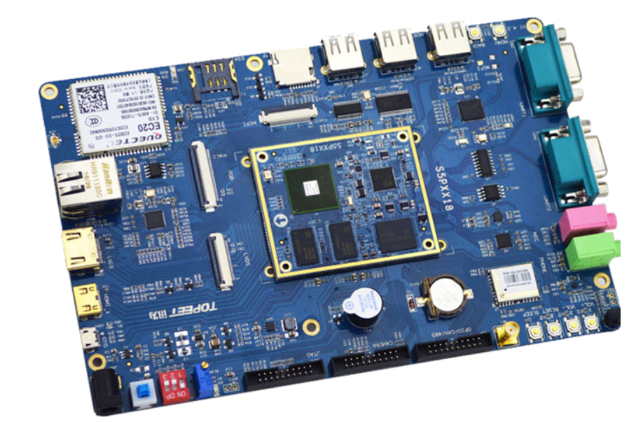
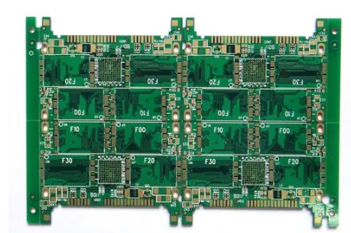
Professional PCB manufacturing and assembly
Building 6, Zone 3, Yuekang Road,Bao'an District, Shenzhen, China
+86-13410863085Mon.-Sat.08:00-20:00

Board surface blistering is one of the more common quality defects in PCB production. Because of the complexity of PCB production process and process maintenance, especially in chemical wet treatment, it is difficult to prevent board surface blistering defects. Based on many years
Board surface blistering is one of the more common quality defects in PCB production. Because of the complexity of PCB production process and process maintenance, especially in chemical wet treatment, it is difficult to prevent board surface blistering defects. Based on many years of practical production experience and service experience, the author briefly analyzes the causes of blistering on the surface of copper plated PCB, hoping that it can play a role in the process production and problem solving!
The blistering on the PCB surface is actually the problem of poor adhesion of the board surface, which is also the problem of the surface quality of the board. This includes two aspects: 1. the cleanliness of the board surface; 2. Surface micro roughness (or surface energy); The blistering problem on all boards can be summarized as the above reasons The binding force between the coatings is poor or too low, which makes it difficult to resist the coating stress, mechanical stress and thermal stress generated in the production and processing process in the subsequent production and processing process and assembly process, and finally causes the separation of the coatings to varying degrees.
Some factors that may cause poor board surface quality during production and processing are summarized as follows:
1. Problems of substrate PCB processing; Especially for some thin substrates (generally less than 0.8mm), due to the poor rigidity of the substrate, it is not suitable to use a brush machine to brush the plate, which may not effectively remove the protective layer specially treated to prevent the oxidation of the copper foil on the plate surface during the production and processing of the substrate. Although this layer is thin and the brush plate is easy to remove, it is difficult to use chemical treatment, so it is important to pay attention to control in production and processing, To avoid the problem of blistering caused by poor adhesion between copper foil and chemical copper; When the thin inner layer is blackened, there will also be problems such as poor blackening and browning, uneven color, and poor local blackening and browning
2. Poor surface treatment caused by oil contamination or other liquid contamination during machining (drilling, laminating, milling, etc.),
3. Poor copper plating brush plate: the pressure of the grinding plate before copper plating is too high, which causes the deformation of the orifice, brush out the copper foil round corner of the orifice, or even leak the base material at the orifice, which will cause blistering at the orifice in the process of copper plating, tin spraying, welding, etc; Even though the brush plate does not cause leakage of the base material, the overweight brush plate will increase the roughness of the copper at the orifice. Therefore, the copper foil at this place is very easy to coarsen during the micro etching process, and there will also be some quality risks; Therefore, attention should be paid to strengthening the control of the brush plate process, and the brush plate process parameters can be adjusted to the best through the abrasion test and water film test;
4. Water washing problem: because the copper plating process needs a lot of chemical water treatment, there are many kinds of acid, alkali, infinite organic and other pharmaceutical solvents, and the board surface is not cleaned by water washing, especially the adjustment of degreaser for copper plating, which will not only cause cross contamination, but also cause local poor treatment or poor treatment effect, uneven defects, and cause some problems in the binding force; Therefore, attention should be paid to strengthening the control of water washing, mainly including the control of water flow, water quality, water washing time, and dripping time of the board; Especially in winter when the temperature is low, the washing effect will be greatly reduced, and more attention should be paid to the control of washing;
5. Micro etching in copper precipitation pretreatment and pattern electroplating pretreatment; Excessive micro etching will cause base material leakage at the orifice and bubble around the orifice; Inadequate micro etching will also lead to insufficient bonding force, leading to blistering; Therefore, it is necessary to strengthen the control of micro etching; Generally, the micro etching depth of pretreatment for copper deposition is 1.5-2 μ m, and the micro etching depth of pretreatment for pattern electroplating is 0.3-1 μ m. If possible, it is better to control the micro etching thickness or rate through chemical analysis and simple test weighing method; Generally, the plate surface after micro etching has bright color, which is uniform pink, without reflection; If the color is uneven or there is reflection, it indicates that there is a potential quality hazard in the pre processing; Pay attention to strengthening inspection; In addition, the copper content, bath temperature, loading capacity and micro etchant content of the micro etching bath should be noted;
7. The plate surface is oxidized during production; If the copperplate is oxidized in the air, it may not only cause no copper in the hole and rough surface, but also cause blistering on the surface; If the copperplate is stored in the acid solution for too long, the surface of the copperplate will also be oxidized, and the oxide film is difficult to remove; Therefore, the copperplate should be thickened in time during the production process, and should not be stored for too long. Generally, the thickening and copper plating should be completed within 12 hours at the latest;
8. Poor reworking of copper sink; Some reworked plates after copper deposition or pattern transformation will blister due to poor plating, incorrect reworking method or improper control of micro etching time during reworking or other reasons; If poor copper deposition is found on the line for rework of copper plate, it can be directly reworked without corrosion after oil removal from the line directly after water washing; It is better not to degrease and slightly erode again; For PCB boards that have been electrically thickened, the micro etching groove should be removed. Pay attention to the time control. You can use one or two boards to roughly calculate the removal time to ensure the removal effect; After deplating, apply a group of soft grinding brushes behind the brush machine to brush lightly and then deposit copper according to the normal production process, but the etching and micro etching time shall be halved or adjusted as necessary;
9. In the process of graphic transfer, insufficient water washing after development, too long time after development or too much dust in the workshop will lead to poor board cleanliness, and poor fiber treatment effect may cause potential quality problems;
10. Before PCB copper plating, the pickling tank should be replaced in time. Too much pollution or too high copper content in the tank solution will not only cause the problem of board cleanliness, but also cause defects such as rough PCB board surface;
11. Organic pollution, especially oil pollution, is likely to occur in the electroplating tank for the automatic line;
12. In addition, in winter, when the bath solution in some PCB factories is not heated, special attention should be paid to the electrification of the plates into the bath during the production process, especially for the plating bath with air agitation, such as copper nickel; For nickel cylinders, it is better to add a warm water to wash the bath before nickel plating in winter (the water temperature is about 30-40 ℃) to ensure that the initial deposition of nickel layer is dense and good;
In the actual production process, there are many reasons for the blistering of the board surface, and the author can only make a brief analysis. For the blistering phenomenon caused by different reasons that may occur in different manufacturers' equipment and technical levels, the specific situation should be analyzed in detail, which can not be generalized, but mechanically copied; The above reason analysis is based on the PCB production process, regardless of primary and secondary importance. This series is just to provide you with a direction to solve problems and a broader vision. The specific situation depends on the on-site situation.


Just upload Gerber files, BOM files and design files, and the KINGFORD team will provide a complete quotation within 24h.