
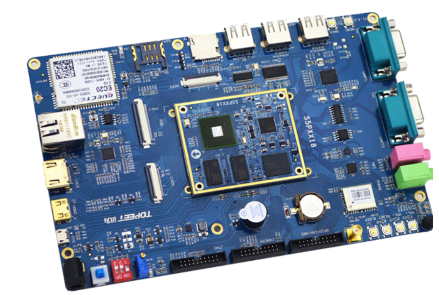
Professional PCB manufacturing and assembly
Building 6, Zone 3, Yuekang Road,Bao'an District, Shenzhen, China
+86-13410863085Mon.-Sat.08:00-20:00

At present, there are four types of lasers used to make micro vias on printed circuit boards: CO 2 laser, YAG laser, excimer laser and copper vapor laser. CO2 lasers are typically used to produce about 75% μ M, but because the light beam will reflect back from the copper surface, it is only suitable for removing the dielectric. CO 2 laser is very neat, cheap and maintenance free. Excimer laser is the best choice to produce high-quality, small diameter holes, and the typical aperture value is less than 10 μ m。 These types are most suitable for high-density array drilling of polyurethane substrate in micro BGA equipment. The development of copper vapor laser is still in its early stage, but it still has the upper hand when high yield is needed. The copper vapor laser can remove the dielectric and copper, but it will bring serious problems in the PCB production process, which will make the air flow can only produce products in a limited environment.

The most common laser used in PCB industry is Q-switched Nd: YAG laser, whose wavelength is 355nm, within the ultraviolet range. This wavelength can melt most metals (Gu, Ni, Au, Ag) when PCB PCB drilling, and its absorption rate exceeds 50% (Meier and Schmidt, 2002). Organic materials can also be melted. The photon energy of the ultraviolet laser can be as high as 3.5 - 7.5 eV, which can break the chemical bond during the melting process, partly through the photochemical action of the ultraviolet laser, and partly through the photothermal action. These functions make UV laser the first choice for PCB industry applications.
The YAG laser system has a laser source, which provides an energy density (flow) of more than 4J/cm2, which is necessary for drilling the copper circulation on the surface of the micro through-hole. The energy density required for the melting process of organic materials is only about 100mJ/cm2, such as epoxy resin and polyurethane. In order to operate accurately in such a wide spectrum range, it is necessary to control the laser energy accurately. The drilling process of the micro through-hole requires two steps. The first step is to open the copper foil with a high energy density laser, and the second step is to remove the dielectric with a low energy density laser.
When the wavelength of the laser is 355nm, the typical spot diameter is about 20 μ m 。 When the pulse time is less than 140 ns, the laser frequency is between 10 - 50 kHz, and the material will not generate heat at this time.
The laser beam is located by the computer controlled scanner/reflection system, and can be focused by the focal aperture lens, so that the beam can drill holes at an accurate angle. The scanning process generates a vector pattern through software to compensate for material and design deviations. The scanning area is 55 x 55mm. This system is compatible with CAM software and supports all commonly used data patterns.
The laser system is proposed by German Mis LPKF. Its mechanical design is based on hard granite, and its surface polishing accuracy is no less than 3 μ m 。 The workbench support is placed on the gas bearing and controlled by the linear generator. The accuracy of positioning is controlled by the glass ruler, and its repeatability is ensured to be within ± 1 μ m 。 The PCB worktable is equipped with optical sensors, which can accurately adjust the laser position at different reflection points to compensate for optical deformation and long-term drift. After adjustment, a series of correction data generated by the software can cover the entire scanning area. Drift scale compensation takes about lmin to operate. Any change of the substrate, such as position deviation from the reference, can be detected by a high-resolution CCD camera and compensated by software control.
This system is very suitable for the production of prototypes. Because it can drill holes and form, it can be used from flexible PCB to rigid PCB, including metal polymers, such as solder resistance, protective layer, dielectric, etc. Raman et al. introduced the most advanced solid-state UV laser system and its application in the production of high-density interconnection micro via.
Lange and Vollrath explained various applications of the ultraviolet laser system (microwire drilling 600 system) in drilling, configuration and cutting. The system can drill holes and micro through-hole, and the copper layer aperture is reduced to 30 μ m. The system can also produce a minimum width of 20 μ The production capacity of the outer layer wire of PCB of M is much higher than that of photochemistry. The production speed of this system can be as high as 250 drilling operations, and can allow all scale inputs, such as Gerber and HPGL. Its operating area is 640 mm x 560 mm (25.2 in x 22 in), and the maximum material height is 50 mm (2 in), which can be used for most commonly used PCB substrates. The base of the machine workbench and its guide rail are made of natural granite with an accuracy of ± 3 μ m 。 PCB worktable is driven by linear driver and supported by air bearing; The position is controlled by a glass ruler with thermal compensation, and its accuracy is soil i μ m 。 The base plate on the console is installed by vacuum equipment.


Just upload Gerber files, BOM files and design files, and the KINGFORD team will provide a complete quotation within 24h.