
Professional PCB manufacturing and assembly
Building 6, Zone 3, Yuekang Road,Bao'an District, Shenzhen, China
+86-13410863085Mon.-Sat.08:00-20:00

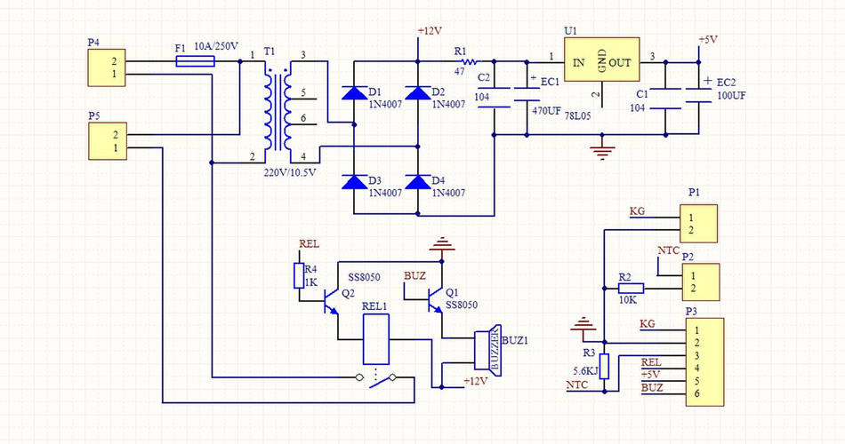
"English Abbreviations" in PCB Production Hardware Schematic Diagram
When PCBA electronic engineers design the schematic diagram, the network label should be as simple as possible. This paper summarizes the basic representation methods for your reference.
1. Common control interface
EN: Enable. Make the chip work. Open the EN pin when you want to use it, and close it when you are not using it. Some chips are high enable and some are low enable, which can only be known according to the specification.
CS: Chip Select. Chip selection. It is usually used to select which chip to receive when sending data. For example, one SPI bus can mount multiple devices, and the DDR bus will also mount multiple DDR memory chips. At this time, CS is required to control which device the data is sent to.
RST: Reset, restart. Sometimes it is simply called R or RESET. Sometimes RST is marked_ N. It indicates that the Reset signal is pulled down to take effect.
INT: Interrupt. As mentioned in the previous article, interruption means someone wakes you up while you are sleeping, or your girlfriend calls while you are watching a movie.
PD: Power Down. It is not necessary to cut off the external power supply of the chip in case of power failure. If the chip has its own PD pin, pulling the PD pin directly is equivalent to power failure. This cable will be used on the camera, because the general camera has three groups of power supply, so it is easier to control the three power supplies and directly cut off the power than to directly operate the PD pin. (There is a Power Delivery called PD in the USB Type-C interface, which is completely different from this one. Don't read it wrong.)
CLK: Clock. The clock line is easy to interfere with others and is also easy to be interfered by others. You need to protect it during layout. For the clock of the digital transmission bus, the nominal value is xxx_ XCLK, such as SPI_ CLK、SDIO_ CLK、I2S_ MCLK (Main Clock), etc. For the system clock, the frequency is often marked. E.g. SYS_ 26M, 32K, etc. It doesn't matter if you mark the number instead of CLK, because only the clock can mark it like this.
CTRL: control. The writing of CONTROL is too long, so it is abbreviated as CTRL, or sometimes CMD (Command) is used.
SW: Switch. SW can be used for signal line switch, key switch, etc.
PWM: PWM, which is very clear.
REF: Reference. E.g. I_ REF,V_ REF, etc. Reference current and reference voltage.
FB:Feedback。 Feedback. There will be feedback signals on the boost and step-down circuits, which are similar in meaning to Reference. The chip dynamically adjusts the output according to the voltage level collected from the outside. If the external voltage is low, increase the output; if the external voltage is high, decrease the output.
A/D: Analog/Digital. For example, DBB=Digital Baseband, AGND=Analog Ground.
D/DATA: Data. SDA (Serial DATA) on I2C and SPI on SPI_ DI、SPI_ DO (Data In, Data Out) and DDR data lines are called D0, D1, D32, etc.
A/Address: Address line. The usage is the same as data line. It is mainly used on the transmission interface with DDR and other addresses and data separated. Other interfaces, such as I2C and SPI in slow speed and MIPI and RJ45 in fast speed, are all transmitted by address and data on a group of lines, so there is no address line.
2. Identification of common directions
TX/RX:Transmit,Receive。 Send and receive. This concept is most widely used on the serial port (UART). One line is responsible for sending and one line is responsible for receiving. Special attention should be paid here that the transmission of one device corresponds to the reception of another device, and the TX should be connected to the RX. If TX is connected to TX and both are sent, data will not be received.
To prevent errors, it can be marked as: UART1_ MRST、UART1_ MTSR。 MasterRX Slave TX. The master is the master chip, and the slave is the slave device. TX and RX are easily mislabeled, especially when the schematic diagram has dozens of pages.
P/N:Positive、Negative。 Positive and negative. Used for differential signal lines. Now there are few parallel data transmission interfaces except DDR and SDIO. USB, LAN, MIPI LCD, Camera, SATA, etc., high-speed data bus has almost become serial data transmission.
The line speed of the serial signal is very high, which can be switched to GHz at random, and the voltage is very low, which is only a few hundred millivolts. Therefore, it is easy to be interfered. It should be made into a differential signal, that is, two lines are used to transmit one data, one positive and one negative. On the other side, the data is subtracted, the interference signal is subtracted, and the negative of the data signal is doubled.
For RESET_ For signals like N, they only play a key role, indicating that the RESET signal is only effective when it is pulled down. Most devices are low effective RESET, and occasionally some devices pull up the RESET.
L/R:Left、Right。 It is usually used for audio cable to distinguish left from right. Sometimes, for example, the signal of the horn is transmitted through differential, that is, SPK_ L_ N、SPK_ L_ P such identification.
3. Abbreviations of common equipment
BB: Baseband, baseband processor. The mobile phone chips of more than ten years ago only have communication functions. There is no such powerful AP (CPU running the system). The main chips in the mobile phone are all called Baseband chips. Later, mobile phones became more powerful. Many old engineers used to call the main chip BB instead of CPU.
P (GPIO)_ 3 In this way. The number of P is the number of GPIOs. P1_ 3 is the third GPIO of the first group. (Different groups of GPIO may have different voltage domains)
BAT: Battery. All battery voltages can be called VBAT.
CHG: Charge.
CAM: Camera.
LCD: display
TP: Touch Panel. (Be careful not to get confused with the Test Point)
DC: Direct Current. It is usually used on equipment as an external DC input interface, rather than power supply mode or voltage. E.g. VCC_ DC_ IN means external DC interface power supply.
The above is the complete set of "English abbreviations" in the pcb production hardware schematic diagram explained by the pcb manufacturer and pcb designer.


Just upload Gerber files, BOM files and design files, and the KINGFORD team will provide a complete quotation within 24h.