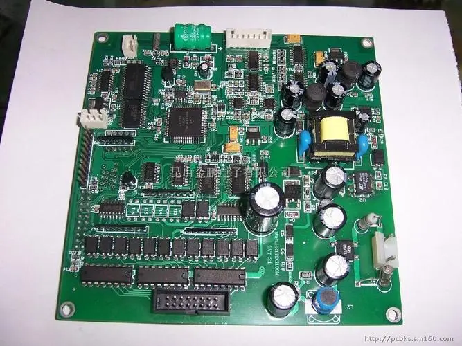
Pcb board design is similar on the surface. It is through the surface that we see the difference, which is critical to the life and function of the printed circuit board.
It is very important for pcb board design to have reliable performance whether in the process of manufacturing assembly or in actual use. In addition to related costs, defects in PCB assembly process may be brought into the final product by the pcb board design, and faults may occur in the actual use process, leading to claims. Therefore, from this point of view, it is no exaggeration to say that the cost of high-quality pcb board design can be ignored.
In all market segments, especially those markets where PCB products are produced in key application fields, the consequences of such failure are unimaginable.

These aspects should be kept in mind when comparing PCBs prices. Although the initial cost of reliable, guaranteed and long-life products is relatively high, it is still worthwhile in the long run.
The 14 most important features of high reliability circuit boards:
1. 25 μ m hole wall copper thickness
Advantages: improved reliability, including the ability to resist Z-axis expansion.
Risk of not doing so:
During actual use, electrical connection problems may occur during hole blowing or degassing, PCB assembly (inner layer separation, hole wall fracture) or failure under load conditions. Ipcc grade (the standard adopted by most factories) requires 20% less copper plating.
2. No welding repair or open circuit repair wire
Advantages: The perfect circuit can ensure reliability and safety without maintenance and risk.
Risk of not doing so:
If the repair is not correct, the circuit board will be cut. Even if the repair is "correct", there is a risk of failure under load conditions (vibration, etc.), This may cause actual use failure.
3. The cleanliness requirements of the instrument panel cluster specifications are exceeded
Advantages: improving the cleanliness of pcb board design can improve the reliability.
Risk of not doing so:
The accumulation of residues and solder on the circuit board will bring risks to the solder mask. Ionic residues will lead to the risk of corrosion and contamination of the welding surface, which may lead to reliability problems (poor solder joints/electrical failures) and ultimately increase the likelihood of actual failures.
4. Strictly control the service life of each surface treatment.
Advantages: weldability, reliability and reduced risk of moisture intrusion.
Risk of not doing so:
Due to the metallographic changes in the surface treatment of old circuit boards, PCB welding problems may occur, and moisture intrusion may cause delamination, separation of inner layers and hole walls (open circuit), and other problems in the assembly process and/or actual use.
5. Use internationally known matrices - do not use "local" or unknown brands
Advantages: Improved reliability and known performance.
Risk of not doing so:
Poor mechanical performance means that the circuit board cannot achieve its expected performance under assembly conditions. For example, high expansion performance will lead to delamination, open circuit and warping problems. Weakening electrical characteristics can lead to poor impedance performance.
6. The tolerance of copper clad plate shall comply with the International Electrotechnical Commission 4101 standard
Advantages: Strictly controlling the thickness of the dielectric layer can reduce the deviation of the expected value of electrical performance.
Risk of not doing so:
The electrical performance may not meet the specified requirements, and the output/performance of the same batch of components will vary greatly.
7. Define welding resistance materials to ensure compliance with IPC-SM-840
Advantages: NCAB Group recognizes "excellent" inks to achieve ink safety and ensure that solder resist inks meet UL standards.
Risk of not doing so:
Poor quality inks can cause problems with adhesion, solder resistance, and hardness. All these problems will lead to the separation of the solder mask from the circuit board, and eventually lead to corrosion of the copper circuit. Poor insulation can cause short circuits due to unexpected electrical connections/arcing.
8. Define tolerances for mechanical features such as shapes, holes, etc
Advantages: strict tolerance control can improve the dimensional quality of products - improving the fit, appearance and function.
Risk of not doing so:
Problems during assembly, such as alignment/fit (problems with press fit pins can only be found when assembly is completed). In addition, due to the increase of dimensional deviation, problems may occur when installing the base.
9. NCAB stipulates the thickness of the solder mask, although the International Chemical Safety Program has no relevant provisions
Advantages: improve electrical insulation, reduce the risk of peeling or loss of adhesion, and enhance resistance to mechanical shock – no matter where the mechanical shock occurs!
Risk of not doing so:
PCB solder mask can cause adhesion, solder resistance and hardness problems. All these problems will lead to the separation of the solder mask from the circuit board, and eventually lead to corrosion of the copper circuit. Poor insulation due to thin solder mask can lead to short circuit due to accidental conduction/arc.
10. Appearance requirements and repair requirements are defined, although the instrument panel cluster is not defined
Advantages: Be careful in the manufacturing process, and be careful to cast safely.
Pcb board design is similar on the surface. It is through the surface that we see the difference, which is critical to the life and function of the printed circuit board.
It is very important for pcb board design to have reliable performance whether in the process of manufacturing assembly or in actual use. In addition to related costs, defects in PCB assembly process may be brought into the final product by the pcb board design, and faults may occur in the actual use process, leading to claims. Therefore, from this point of view, it is no exaggeration to say that the cost of high-quality pcb board design can be ignored.
In all market segments, especially those markets where PCB products are produced in key application fields, the consequences of such failure are unimaginable.
These aspects should be kept in mind when comparing PCBs prices. Although the initial cost of reliable, guaranteed and long-life products is relatively high, it is still worthwhile in the long run.
The 14 most important features of high reliability circuit boards:
1. 25 μ m hole wall copper thickness
Advantages: improved reliability, including the ability to resist Z-axis expansion.
Risk of not doing so:
During actual use, electrical connection problems may occur during hole blowing or degassing, PCB assembly (inner layer separation, hole wall fracture) or failure under load conditions. Ipcc grade (the standard adopted by most factories) requires 20% less copper plating.
2. No welding repair or open circuit repair wire
Advantages: The perfect circuit can ensure reliability and safety without maintenance and risk.
Risk of not doing so:
If the repair is not correct, the circuit board will be cut. Even if the repair is "correct", there is a risk of failure under load conditions (vibration, etc.), This may cause actual use failure.
3. The cleanliness requirements of the instrument panel cluster specifications are exceeded
Advantages: improving the cleanliness of pcb board design can improve the reliability.
Risk of not doing so:
The accumulation of residues and solder on the circuit board will bring risks to the solder mask. Ionic residues will lead to the risk of corrosion and contamination of the welding surface, which may lead to reliability problems (poor solder joints/electrical failures) and ultimately increase the likelihood of actual failures.
4. Strictly control the service life of each surface treatment.
Advantages: weldability, reliability and reduced risk of moisture intrusion.
Risk of not doing so:
Due to the metallographic changes in the surface treatment of old circuit boards, PCB welding problems may occur, and moisture intrusion may cause delamination, separation of inner layers and hole walls (open circuit), and other problems in the assembly process and/or actual use.
5. Use internationally known matrices - do not use "local" or unknown brands
Advantages: Improved reliability and known performance.
Risk of not doing so:
Poor mechanical performance means that the circuit board cannot achieve its expected performance under assembly conditions. For example, high expansion performance will lead to delamination, open circuit and warping problems. Weakening electrical characteristics can lead to poor impedance performance.
6. The tolerance of copper clad plate shall comply with the International Electrotechnical Commission 4101 standard
Advantages: Strictly controlling the thickness of the dielectric layer can reduce the deviation of the expected value of electrical performance.
Risk of not doing so:
The electrical performance may not meet the specified requirements, and the output/performance of the same batch of components will vary greatly.
7. Define welding resistance materials to ensure compliance with IPC-SM-840
Advantages: NCAB Group recognizes "excellent" inks to achieve ink safety and ensure that solder resist inks meet UL standards.
Risk of not doing so:
Poor quality inks can cause problems with adhesion, solder resistance, and hardness. All these problems will lead to the separation of the solder mask from the circuit board, and eventually lead to corrosion of the copper circuit. Poor insulation can cause short circuits due to unexpected electrical connections/arcing.
8. Define tolerances for mechanical features such as shapes, holes, etc
Advantages: strict tolerance control can improve the dimensional quality of products - improving the fit, appearance and function.
Risk of not doing so:
Problems during assembly, such as alignment/fit (problems with press fit pins can only be found when assembly is completed). In addition, due to the increase of dimensional deviation, problems may occur when installing the base.
9. NCAB stipulates the thickness of the solder mask, although the International Chemical Safety Program has no relevant provisions
Advantages: improve electrical insulation, reduce the risk of peeling or loss of adhesion, and enhance resistance to mechanical shock – no matter where the mechanical shock occurs!
Risk of not doing so:
PCB solder mask can cause adhesion, solder resistance and hardness problems. All these problems will lead to the separation of the solder mask from the circuit board, and eventually lead to corrosion of the copper circuit. Poor insulation due to thin solder mask can lead to short circuit due to accidental conduction/arc.
10. Appearance requirements and repair requirements are defined, although the instrument panel cluster is not defined
Advantages: Be careful in the manufacturing process, and be careful to cast safely.


