
Professional PCB manufacturing and assembly
Building 6, Zone 3, Yuekang Road,Bao'an District, Shenzhen, China
+86-13410863085Mon.-Sat.08:00-20:00

Not all products are cheaper with less or smaller components. Just like chips at this stage, the smaller the area, the more expensive it is. The same is true for PCB boards. It does not mean that the thinner the product is, the cheaper it is. Similarly, the cost will be lower if one layer is added.
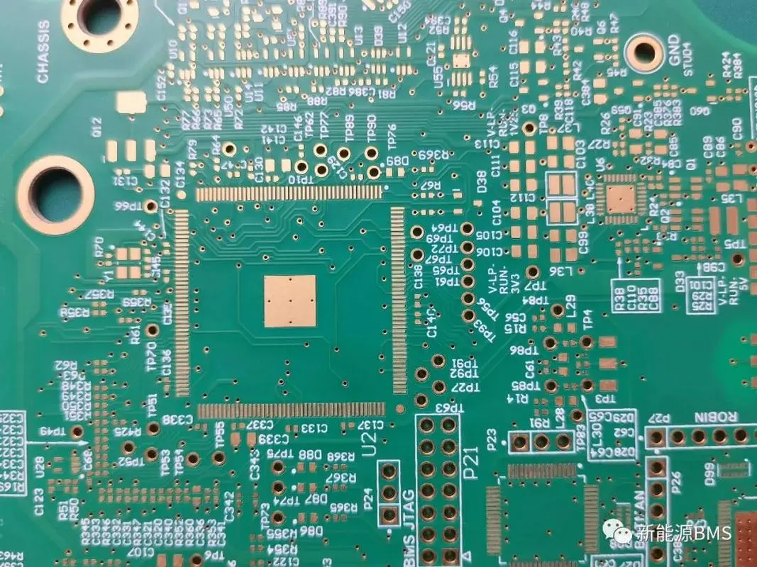
Pcb circuit board has two different structures: core structure and foil structure.
In the core structure, all conductive layers in the circuit board are laid on the core material; In the foil structure, only the internal conductive layer of the circuit board is applied to the core material, and the external conductive layer is applied to the foil dielectric plate. All conductive layers are bonded together by a multilayer lamination process through a dielectric.
Nuclear material is the double-sided foil coating in the factory. Because each core has two sides, when fully utilized, the number of conductive layers of PCB is even. Why not use foil on one side and nuclear structure on the other? The main reasons are: PCB cost and PCB bending.
Cost advantages of even layer circuit boards
Because there is one less layer of medium and foil, the raw material cost of odd PCB is slightly lower than that of even PCB, but the processing cost of odd PCB is significantly higher than that of even PCB. The processing cost of inner layer is the same; However, the foil/core structure obviously increases the processing cost of the outer layer.
On the basis of core structure process, non-standard laminated core layer bonding process should be added to odd PCB. Compared with the core structure, the production efficiency of the factory adding foil outside the core structure will decrease. Before laminating and bonding, the outer core requires additional process treatment, which increases the risk of outer layer being scratched and etched incorrectly.
Having seen the above contents, I believe many people should understand that in fact, the thinner the PCB is, the cheaper it is. It is defined according to different products. Perhaps a certain PCB product will be much cheaper after reducing the area or cost. However, as a PCB technical product, the functionality of electronic products is still very different.
What is a PCB half orifice?
The definition of metal half hole (groove) is that one hole is drilled and then drilled again, and the shape process will eventually retain half of the metallized hole (groove), which is simply to cut half of the plate edge metallized hole,
Pcb, such as copper burrs on the hole wall, has been a difficult problem in the processing.
This kind of PCB with a whole row of semi metallized holes on the edge of the board is characterized by its small aperture, which is mostly used on the carrier board. As a sub board of a motherboard, these semi metallized holes are welded together with the PCB motherboard and the pins of PCB components.
Therefore, if there are copper burrs left in these semi metallized holes, when the plug-in manufacturer conducts welding, it will lead to insecure solder legs and faulty soldering, and in serious cases, it will cause bridging short circuit between two pins.
Whether drilling or milling, the rotation direction of SPINDLE is clockwise. Since the copper attached to the PCB hole wall has no adhesion support, when the tool moves forward, the metallized layer in the hole affected by external force will curl with the rotation direction of the tool, resulting in copper barb warping and residue.


Just upload Gerber files, BOM files and design files, and the KINGFORD team will provide a complete quotation within 24h.