
Professional PCB manufacturing and assembly
Building 6, Zone 3, Yuekang Road,Bao'an District, Shenzhen, China
+86-13410863085Mon.-Sat.08:00-20:00

1. What is COB soft package
Careful attention may find that there is a lump of black things on some circuit boards, so what is this thing? Why does it play a role on the circuit board? In fact, it is a kind of packaging, which we often call "soft packaging". It is said that the soft packaging is actually for "hard", and its composition material is epoxy resin. We usually see that the receiving surface of the receiver is also this material, and its inside is a chip IC. This process is called "Bonding", and we usually call it "binding".
This is a wiring process in the chip production process. Its English name is COB (Chip On Board), that is, chip on board packaging. It is one of the bare chip mounting technologies. The chip is mounted on the HDI PCB printed circuit board using epoxy resin. Why do some circuit boards not have this packaging? What are the characteristics of this packaging?
2. COB Soft Package Features
This kind of soft packaging technology is often for cost. As the simplest bare chip mounting, in order to protect the internal IC from damage, this kind of packaging generally requires one-time molding, which is generally placed on the copper foil surface of the circuit board. The shape is round and the color is black. This kind of packaging technology has the advantages of low cost, space saving, thinness, good heat dissipation, simple packaging method, etc. Many integrated circuits, Especially for most low-cost circuits, it is only necessary to lead more than one metal wire on the integrated circuit chip in this way, and then submit it to the manufacturer to put the chip on the circuit board, weld it with a machine, and then glue it to harden.
3. Application occasions
Because of its unique characteristics, this packaging is also used in some electronic circuit circuits, such as MP3 players, electronic organs, digital cameras, game consoles, etc.
In fact, COB soft packaging is not only limited to chips, but also widely used in LED. For example, COB light source is an integrated surface light source technology that is directly attached to the mirror metal substrate on the LED chip.
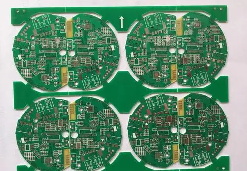
Pay attention to these matters during PCB fastboard proofing
Usually, enterprises will produce small samples for testing before conducting PCB production, which is also known as rapid PCB proofing. Now there are many manufacturers specializing in pcb proofing, and enterprises can choose appropriate pcb manufacturers for cooperation according to their own product needs. So, do you know what should be paid attention to in the process of rapid PCB proofing? The following precautions are summarized in the small section:
1、 Note the number of PCB samples
For enterprises with large demand, a batch of used for testing also occupy the cost of the enterprise. Especially for enterprises with many types and large quantities, the cost of pcb proofing and testing is relatively high. Enterprises should note that the number of PCB proofing can also reduce some production costs.
2、 Pay attention to confirm the device packaging
It is a process in the PCB manufacturing process that the chip with a specific role in PCB welding is packaged with a shielding cover. In the process of rapid PCB proofing, enterprises should pay attention to whether the internal chips and electronic components are wrongly soldered during packaging to ensure the quality of PCB proofing, so that normal detection function and subsequent PCB batch production can be achieved.
3、 Pay attention to the overall electrical inspection
After completing the rapid proofing of PCB boards, enterprises should conduct a comprehensive electrical inspection on the template to ensure that every function and every detail of the circuit board meet the expected effect. Ensure that there is no or very little defective rate in subsequent mass production.


Just upload Gerber files, BOM files and design files, and the KINGFORD team will provide a complete quotation within 24h.