
Professional PCB manufacturing and assembly
Building 6, Zone 3, Yuekang Road,Bao'an District, Shenzhen, China
+86-13410863085Mon.-Sat.08:00-20:00

Design Guidelines for Mixed Signal Boards
Mixed-Signal Circuit Layout Basics When digital and analog circuits share the same components on the same board, the layout and routing of the circuit must be methodical.
In mixed-signal PCB design, there are special requirements for power traces and the isolation of analog noise and digital circuit noise to avoid noise coupling, which increases the complexity of layout and routing. The special demands on power transmission lines and the requirement to isolate noise coupling between analog and digital circuits add further complexity to the layout and routing of mixed-signal PCBs.
If the power supply of the analog amplifier in the A/D converter and the digital power supply of the A/D converter are connected together, it is likely to cause mutual influence between the analog part and the digital part circuit. Perhaps, because of the location of the I/O connectors, the layout scheme must mix the routing of digital and analog circuits.
Before placing and routing, engineers need to understand the fundamental weaknesses of the placement and routing scheme. Even with false positives, most engineers tend to use placement and routing information to identify potential electrical effects.
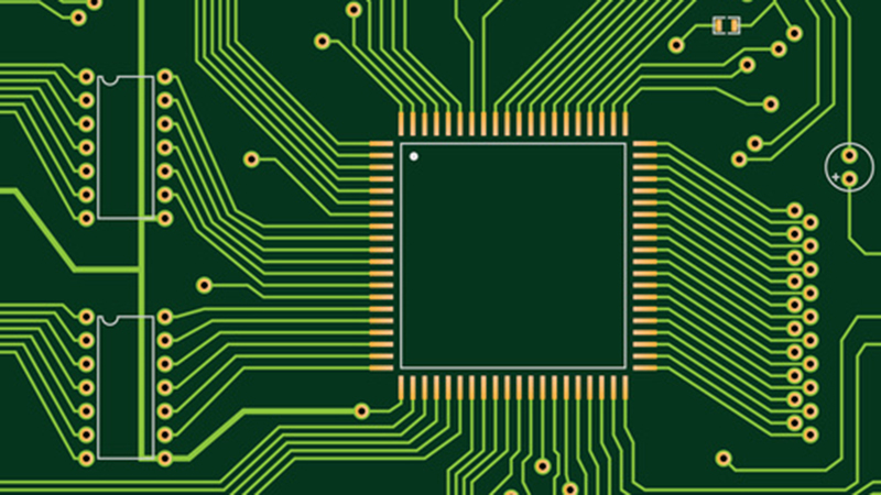
Layout and routing of modern mixed-signal PCBs
The following will illustrate the technology of mixed signal PCB layout and wiring through the design of OC48 interface card. OC48 stands for Optical Carrier Standard 48, basically oriented to 2.5Gb serial optical communication, which is a kind of high-capacity optical communication standard in modern communication equipment. The OC48 interface card includes several typical mixed-signal PCB layout and routing issues, and its layout and routing process will indicate the order and steps to solve the mixed-signal PCB layout scheme.
The OC48 card contains an optical transceiver that realizes bidirectional conversion of optical signals and analog electrical signals. Analog signal input or output digital signal processor, DSP converts these analog signals into digital logic level, which can be connected with microprocessor, programmable gate array and system interface circuit of DSP and microprocessor on OC48 card . A separate phase-locked loop, mains filter and local voltage reference are also integrated.
Among them, the microprocessor is a multi-power supply device, the main power supply is 2V, and the I/O signal power supply of 3.3V is shared by other digital devices on the board. Independent digital clock sources provide clocks for OC48I/O, microprocessor and system I/O.
After checking the layout and wiring requirements of different functional circuit blocks, it is initially recommended to use a 12-layer board, as shown in Figure 3. Microstrip and stripline layer configurations safely reduce coupling to adjacent trace layers and improve impedance control. A ground plane between the first and second layers will isolate the sensitive analog reference source, CPU core, and PLL filter power routing from the microprocessor and DSP devices on the first layer. The power and ground planes always come in pairs, as is done on the OC48 card for the shared 3.3V power plane. This will lower the impedance between the power supply and ground, thereby reducing noise on the power supply signal.
It is necessary to avoid running digital clock lines and high-frequency analog signal lines near the power plane, otherwise, the noise of the power signal will be coupled into the sensitive analog signal.
Carefully consider utilizing power and analog ground plane splits, especially at the input and output of mixed-signal devices, according to digital signal routing needs. Routing through an opening on an adjacent signal layer can cause impedance discontinuities and poor transmission line loops. These can cause signal quality, timing and EMI problems.
Sometimes adding several ground planes, or using several peripheral layers under a device for the local power plane or ground plane, can eliminate openings and avoid the above problems. Multiple ground planes are used on the OC48 interface card. Maintaining the lamination symmetry of the position of the opening layer and the wiring layer can avoid deformation of the card and simplify the manufacturing process. Due to the strong ability of 1 ounce copper clad laminate to withstand large currents, 1 ounce copper clad laminate should be used for the 3.3V power supply layer and the corresponding ground layer, and 0.5 ounce copper clad laminate can be used for other layers. In this way, the transient high current or peak period can be reduced. Voltage fluctuations.
If you are designing a complex system from the ground plane up, use 0.093-inch and 0.100-inch thick cards to support the wiring and ground isolation planes. The card thickness must also be scaled to the routing feature dimensions of the via pads and holes so that the aspect ratio of the drilled hole diameter to the thickness of the finished card does not exceed the aspect ratio of the metallized holes provided by the manufacturer.
If you want to design a low-cost, high-volume commercial product with a minimum number of routing layers, carefully consider the routing details of all special power supplies on the mixed-signal PCB before placing or routing. Have the target manufacturer review the preliminary layering scheme before starting place and route. Layering is basically based on finished product thickness, number of layers, copper weight, impedance (with tolerance) and minimum via pad and hole size, and the manufacturer should provide layering recommendations in writing.
Recommendations include all controlled-impedance stripline and microstrip configuration examples. Consider your impedance predictions in conjunction with the manufacturer's impedance predictions. These impedance predictions can then be used to validate signal routing characteristics in the simulation tools used to develop CAD routing rules.
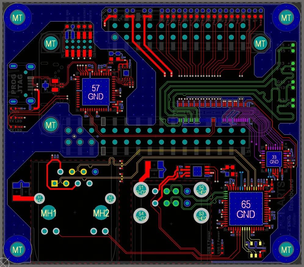
OC48 Card Layout
High-speed analog signals between optical transceivers and DSPs are very sensitive to external noise. Also, all the special power and reference voltage circuitry creates a lot of coupling between the card's analog and digital power delivery circuits. Sometimes, limited by the shape of the case, high-density boards have to be designed. Due to the orientation of the external optical cable access card and the high size of some components of the optical transceiver, the position of the transceiver in the card is largely fixed. System I/O connector locations and signal assignments are also fixed. This is the basic work that must be done before layout (see Figure 4).
As with most successful high-density analog placement and routing schemes, placement meets routing requirements, and placement and routing requirements must be balanced. The "place and route" approach is not recommended for the analog portion of a mixed-signal PCB and the local CPU core operating at 2V. For the OC48 card, the part of the DSP analog circuit that includes the analog reference voltage and the bypass capacitor of the analog power supply should be interactively wired first. After the wiring is completed, the entire DSP with analog components and wiring should be placed close enough to the optical transceiver to fully ensure the shortest wiring length, bends and vias from the high-speed analog differential signal to the DSP. Symmetry in differential placement and routing will reduce the effects of common-mode noise. However, it is difficult to predict the best solution for placement before routing
Consult the chip distributor for the design guidelines of the PCB layout. Before designing according to the guidelines, fully communicate with the distributor's application engineer. Many chip distributors have strict time constraints on providing high-quality layout advice. Sometimes, they provide a solution that is feasible for the "Tier 1 Customer" using the device. In the field of signal integrity (SI) design, the signal integrity design of new devices is particularly important. Using the distributor's basic guidelines combined with specific requirements for each power and ground pin in the package, layout and routing of the OC48 card with integrated DSP and microprocessor can begin.
Once the location and routing of the high-frequency analog section is determined, the rest of the digital circuitry can be placed according to the groupings shown in the block diagram. Attention should be paid to the careful design of the following circuits: the position of the PLL power supply filter circuit in the CPU with high sensitivity to analog signals; the local CPU core voltage regulator; the reference voltage circuit for the "digital" microprocessor.
This is when the electrical and manufacturing guidelines for digital wiring can be properly applied to the design. The foregoing design of signal integrity for high-speed digital buses and clock signals reveals some special wiring topology requirements for processor bus, balanced Ts, and skew matching of certain clock signal wiring. But you may not know, there are also newer suggestions, that is, to add some termination resistors.
In the process of solving the problem, it is a matter of course to make some adjustments in the layout stage. However, before starting routing, it is an important step to verify the timing of the digital section according to the layout scheme. At this point, a full DFM/DFT layout review of the board will help ensure that the card meets the customer's needs.
Digital Wiring for OC48 Cards
For digital device power lines and digital parts of mixed-signal DSPs, digital routing begins with SMD escape patterns. The shortest and widest traces allowed by the assembly process should be used. For high-frequency devices, the printed line of the power supply is equivalent to a small inductor, which will worsen the noise of the power supply and cause undesired coupling between analog and digital circuits. The longer the power trace, the greater the inductance.
Optimal placement and routing schemes can be obtained by using digital bypass capacitors. In short, fine-tune the location of the bypass capacitors as needed, making them easy to install and distribute around the digital parts and the digital portion of the mixed-signal device. The same "shortest and widest traces" approach should be used to route the bypass capacitor exit diagram.
When the power branch is to cross a continuous plane (such as the 3.3V power plane on the OC48 interface card), then the power pin and the bypass capacitor itself do not have to share the same exit map to get the lowest inductance and ESR bypass. On a mixed-signal PCB such as the OC48 interface card, special attention must be paid to the routing of the power branch. Remember to place additional bypass capacitors in a matrix arrangement across the card, even near passive components
After the power outlet diagram is determined, automatic wiring can begin. The ATE test contacts on the OC48 card should be defined during logic design. Make sure ATE touches 100% of the nodes. In order to implement ATE testing with a minimum ATE test probe of 0.070 inches, the position of the breakout via must be reserved to ensure that the power plane is not interrupted by the antipads crossing of the via.
If a power and ground layer opening (split) scheme is to be used, the offset layer (layer bias) should be selected on the adjacent wiring layer parallel to the opening. On the adjacent layer, the forbidden wiring area is defined according to the perimeter of the opening area to prevent wiring from entering. If routing must pass through the open area to another layer, ensure that the other layer adjacent to the routing is a continuous ground plane. This will reduce reflection paths. Having bypass capacitors across open power planes is beneficial for some digital signal layouts, but bridging between digital and analog power planes is not recommended because noise couples to each other through the bypass capacitors.
Several of the latest automated routing applications are capable of routing high-density, multilayer digital circuits. In the initial routing stage, use a large via spacing of 0.050 inches in the SMD outlet and consider the package type used. The subsequent routing stage should allow the vias to be placed closer to each other, so that all tools can achieve the highest routing rate. and the lowest via count. Since the OC48 processor bus adopts an improved star topology, it has the highest priority in automatic routing.
Summarize
After the OC48 card board is completed, signal integrity verification and timing simulation should be carried out. The simulation proves that the routing guidance meets the expected requirements and improves the timing index of the second layer bus. Finally, the design rule check, final manufacturing review, mask and review are performed and issued to the fabricator, and the layout task is officially ended.


Just upload Gerber files, BOM files and design files, and the KINGFORD team will provide a complete quotation within 24h.