
Professional PCB manufacturing and assembly
Building 6, Zone 3, Yuekang Road,Bao'an District, Shenzhen, China
+86-13410863085Mon.-Sat.08:00-20:00

RF circuit PCB design processing skills
Since the radio frequency (RF) circuit is a distributed parameter circuit, it is easy to produce skin effect and coupling effect in the actual work of the circuit, so in the actual PCB design, it will be found that the interference radiation in the circuit is difficult to control, such as: digital circuit and analog Interference between circuits, noise interference of power supply, interference caused by unreasonable ground wire, etc. Because of this, how to weigh the pros and cons to find a suitable compromise point in the PCB design process, reduce these interferences as much as possible, and even avoid the interference of some circuits is the key to the success of RF circuit PCB design. From the perspective of PCB LAYOUT, this paper provides some processing skills, which are of great use in improving the anti-interference ability of radio frequency circuits.
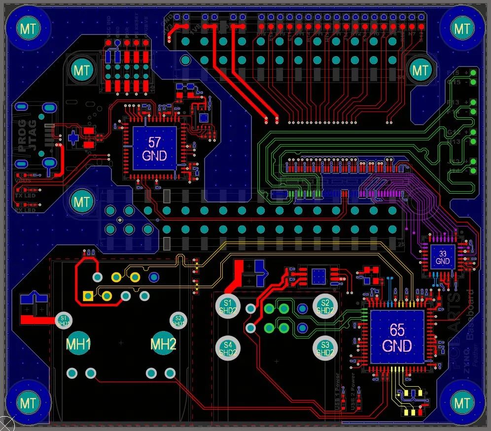
1. RF layout
The main discussion here is the layout of the components of the multilayer board. The key to component location layout is to fix components located on the RF path, by adjusting their orientation, minimize the length of the RF path, and keep the input away from the output, separating high-power circuits and low-power circuits as far as possible, sensitive analog Signals away from high-speed digital signals and RF signals.
The following techniques are often used in layout.
1.1 One-line layout
The components of the RF main signal should adopt a straight layout as much as possible, as shown in Figure 1. However, due to the limitation of the space of the PCB board and the cavity, it is often impossible to arrange in a straight line. At this time, an L-shaped layout can be used instead of a U-shaped layout (as shown in Figure 2). Sometimes it is unavoidable. It is possible to increase the distance between the input and output, at least 1.5cm.
In addition, when adopting an L-shaped or U-shaped layout, it is best not to turn at the turning point as soon as it enters the interface, as shown in the left of Figure 3, but to turn after a slight straight line, as shown in the right of Figure 3.
1.2 Same or symmetrical layout
The same modules should be made into the same or symmetrical layout as much as possible, as shown in Figure 4 and Figure 5.
1.3 Cross layout
The feed inductance of the bias circuit is placed perpendicular to the RF channel, as shown in Figure 6, mainly to avoid mutual inductance between inductive devices.
1.4 45 degree layout
In order to make reasonable use of space, the device can be laid out in a 45-degree direction to make the radio frequency line as short as possible.
2. RF wiring
The overall requirements for wiring are: RF signal traces are short and straight, reducing line mutations, punching fewer vias, not intersecting with other signal lines, and adding as many vias as possible around the RF signal lines.
The following are some commonly used optimization methods:
2.1 Gradient line processing
In the case that the radio frequency line width is much larger than the IC device pin width, the line width of the contact chip adopts a gradual change method,
2.2 Arc processing
If the RF line cannot be straight, it should be treated as a circular arc line, which can reduce the external radiation and mutual coupling of RF signals. Experiments have proved that the corner of the transmission line adopts a curved right angle, which can minimize the return loss. As shown in Figure 9.
2.3 Ground and Power
Make the ground wire as thick as possible. If conditions permit, each layer of the PCB should be grounded as much as possible, and the ground should be connected to the main ground, and more ground vias should be drilled to reduce the ground impedance as much as possible.
The power supply of the RF circuit should not be divided into planes as much as possible. The whole power plane not only increases the radiation of the power plane to the RF signal, but is also easily interfered by the RF signal. Therefore, the power line or plane is generally in the shape of a long strip, and it is processed according to the size of the current. It is as thick as possible under the premise of meeting the current capacity, but it cannot be widened without limit. When handling power cords, be sure to avoid loops.
The direction of the power line and the ground line should be parallel to the direction of the RF signal but not overlapped. Where there is a cross, it is best to use a vertical cross.
2.4 Cross processing
The RF signal and the IF signal traces are crossed, and a ground is separated between them as much as possible.
When the RF signal crosses other signal traces, try to arrange a layer of ground connected to the main ground along the RF trace between them. If not possible, make sure they are criss-crossed. Other signal traces here also include power lines.
2.5 Land parcel processing
Ground-covering processing of radio frequency signals, interference sources, sensitive signals and other important signals can not only improve the anti-interference ability of the signal, but also reduce the interference of the signal to other signals. As shown in Figure 10.
2.6 Copper Foil Treatment
The copper foil treatment is required to be smooth and flat, and no long lines or sharp corners are allowed. If it cannot be avoided, a few ground vias should be filled at the sharp corners, slender copper foil or the edge of the copper foil.
2.7 Spacing processing
The radio frequency line must be at least 3W wide from the edge of the adjacent ground plane, and there must be no non-ground vias within the 3W range.
The radio frequency lines on the same layer should be covered with ground, and ground via holes should be added on the ground copper skin. The hole spacing should be less than 1/20 of the wavelength (λ) corresponding to the signal frequency, and they should be evenly arranged. The edge of the ground copper skin is 2W wide or 3H high from the radio frequency line, and H represents the total thickness of the adjacent dielectric layer.
3. Cavity treatment
For the entire RF circuit, the RF units of different modules should be isolated with a cavity, especially between sensitive circuits and strong radiation sources. In high-power multi-stage amplifiers, the isolation between stages should also be ensured. After the tributary of the entire circuit is placed, it is the treatment of the shielding cavity. The following precautions are required for the treatment of the shielding cavity:
The entire shielding cavity should be made into a regular shape as far as possible, which is convenient for molding. For each shielding cavity, make it as rectangular as possible, and avoid square shielding cavity.
The corners of the shielding cavity are arc-shaped, and the shielding metal cavity is generally cast, and the arc-shaped corners are convenient for drafting during casting. As shown in Figure 12.
The periphery of the shielding cavity is sealed, and the interface wires are generally introduced into the cavity using stripline or microstrip lines, while different modules inside the cavity use microstrip lines, and slots are used to connect different cavities. The width of the slot It is 3mm, and the microstrip line is in the middle.
3mm metallized holes are placed at the corners of the cavity to fix the shielding shell, and the same metallized holes are evenly placed on each long cavity to strengthen the support.
The cavity is generally treated with window opening, which is convenient for welding the shielding shell. The thickness of the cavity is generally more than 2 mm. Two rows of window via screens are added to the cavity. The vias are staggered from each other, and the distance between the same row of vias is 150MIL.
4 Conclusion
The key to the success or failure of RF circuit PCB design lies in how to reduce circuit radiation, thereby improving the anti-interference ability, but in the actual layout and wiring, the handling of some problems is in conflict, so how to find a compromise point to make the whole RF circuit integrated Optimal performance is a problem that designers must consider. All of these require the designer to have certain practical experience and engineering design ability, but to have these abilities, every designer cannot achieve it overnight. In order to continue to improve. This article summarizes some design experience in the work, which is conducive to improving the anti-interference ability of RF circuit PCB, and helping beginners in RF circuit design to avoid unnecessary detours.
Four basic characteristics of PCB RF circuit
Here, the four basic characteristics of RF circuits will be interpreted from four aspects: RF interface, small desired signal, large interference signal, and interference of adjacent channels, and important factors that need special attention in the PCB design process are given.
RF interface for RF circuit simulation
Conceptually, wireless transmitters and receivers can be divided into two parts: baseband and radio frequency. The fundamental frequency includes the frequency range of the transmitter's input signal, as well as the frequency range of the receiver's output signal. The bandwidth of the fundamental frequency determines the basic rate at which data can flow in the system. The fundamental frequency is used to improve the reliability of the data stream and reduce the load imposed by the transmitter on the transmission medium under a specific data transmission rate. Therefore, a large amount of signal processing engineering knowledge is required when designing a baseband circuit on a PCB. The RF circuit of the transmitter converts the processed baseband signal, upconverts it to a designated channel, and injects this signal into the transmission medium. In contrast, the receiver's RF circuitry takes the signal from the transmission medium, converts it, and downconverts it to the base frequency.
Transmitters have two main PCB design goals: the first is that they must transmit a certain amount of power while dissipating the least amount of power possible. The second is that they cannot interfere with the normal operation of transceivers in adjacent channels. As far as receivers are concerned, there are three main PCB design goals: first, they must accurately reproduce small signals; second, they must be able to remove interfering signals outside the desired channel; and lastly, like transmitters, the power they consume must very small.
Large interference signal for RF circuit simulation
The receiver must be sensitive to small signals even in the presence of large interfering signals (blockers). This occurs when trying to receive a weak or distant transmission while there is a powerful transmitter nearby broadcasting on an adjacent channel. The interfering signal may be 60~70 dB larger than the expected signal, and can block the reception of the normal signal by covering the input stage of the receiver with a large amount of way, or causing the receiver to generate an excessive amount of noise at the input stage. The above two problems can occur if the receiver is driven into a non-linear region by an interfering source at the input stage. To avoid these problems, the front end of the receiver must be very linear.

Therefore, "linearity" is also an important consideration when designing a receiver on a PCB. Since the receiver is a narrow-band circuit, the non-linearity is counted by measuring "intermodulation distortion". This involves driving an input signal with two sine or cosine waves of similar frequency, in-band, and then measuring the product of their intermodulations. Generally speaking, SPICE is a time-consuming and cost-intensive simulation software, because it must perform many cycles of calculations to obtain the required frequency resolution to understand the distortion.
Small Desired Signals for RF Circuit Simulation
The receiver must be sensitive to small input signals. Generally speaking, the input power of the receiver can be as small as 1 μV. A receiver's sensitivity is limited by the noise generated by its input circuitry. Therefore, noise is an important consideration when designing a receiver on a PCB. Also, the ability to predict noise with simulation tools is essential. Figure 1 is a typical superheterodyne receiver. The received signal is first filtered, and then the input signal is amplified by a low noise amplifier (LNA). This signal is then mixed with a first local oscillator (LO) to convert the signal to an intermediate frequency (IF). The noise performance of the front-end circuit mainly depends on the LNA, mixer (mixer) and LO. While it is possible to find noise in the LNA using traditional SPICE noise analysis, it is useless for mixers and LOs because the noise in these blocks is heavily influenced by the large LO signal.
A small input signal requires that the receiver must have a great amplification function, usually such a high gain of 120 dB is required. At such high gains, any signal that couples from the output back into the input can cause problems. An important reason for using a superheterodyne receiver architecture is that it spreads the gain over several frequencies to reduce the chance of coupling. This also makes the frequency of the first LO different from that of the input signal, which prevents large interfering signals from "contaminating" the small input signal.
For different reasons, direct conversion or homodyne architectures can replace superheterodyne architectures in some wireless communication systems. In this architecture, the RF input signal is converted directly to the fundamental frequency in a single step, therefore, most of the gain is in the fundamental frequency, and the LO is at the same frequency as the input signal. In this case, the influence of small amounts of coupling must be understood and a detailed model of "stray signal paths" such as coupling through the substrate, package pins and bond wires must be established (bondwire) between the coupling, and coupling through the power line.
Interference of Adjacent Channels in Radio Frequency Circuit Simulation
Distortion also plays an important role in transmitters. The non-linearity produced by the transmitter in the output circuit may spread the bandwidth of the transmitted signal in adjacent channels. This phenomenon is called "spectral regrowth". Before the signal reaches the transmitter's power amplifier (PA), its bandwidth is limited; however, "intermodulation distortion" within the PA causes the bandwidth to increase again. If the bandwidth is increased too much, the transmitter will not be able to meet the power requirements of its adjacent channels. When transmitting digitally modulated signals, it is practically impossible to use SPICE to predict spectral regrowth. Because there are about 1000 digital symbol (symbol) transmission operations must be simulated to obtain a representative spectrum, and also need to combine high frequency carrier
Design Guidelines for Mixed Signal Boards
May 31,2023


Just upload Gerber files, BOM files and design files, and the KINGFORD team will provide a complete quotation within 24h.