
Professional PCB manufacturing and assembly
Building 6, Zone 3, Yuekang Road,Bao'an District, Shenzhen, China
+86-13410863085Mon.-Sat.08:00-20:00

Design to Handle RF PCBs
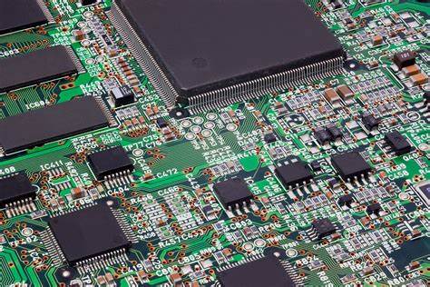
A radio frequency (RF) printed circuit board is a very high-speed circuit that operates at frequencies of 100mhz and above, typically between 500mhz and 2ghz. RF pcbs are the backbone of high-tech devices such as wireless networks, smartphones, smart TVs, and more. Furthermore, RF PCBs are used in automotive, medical equipment, military and aerospace applications for proficient measurement, detection and monitoring functions.
RF circuits differ significantly from any typical analog and digital circuits. RF signals include high-frequency analog signals that can be at any voltage or current level, within set limits, at any given point in time. The design of this RF PCB is quite complex and strict guidelines must be followed to mitigate interference problems caused by high frequency signals.
During the RF PCB design process, one of the most frequently discussed topics is how to select the proper material for the target application to influence the final design. The selected substrate material determines the price, thickness, circuit layout, mounting possibilities, etc., covering a large part of the overall product functionality.
Guide: Choosing the Right Laminate Substrate for High Frequency RF PCB Applications
Dielectric constant (Dk) matching of the resin and substrate weave material is strongly recommended. Inhomogeneous Dks in the substrate can cause problems in high frequency operation. In PCB design, the designer must ensure that the Dk matches for all substrate layers.
The degree to which the substrate expands with temperature changes during PCB manufacturing or operation is known as the coefficient of thermal expansion. Different layers of a laminated substrate may expand at different rates, leading to functional failures and reliability issues. In RF PCB design, matching CTEs of all substrate layers is a must.
Choosing a tight mesh of laminated substrates with weaving properties is recommended as it may directly affect Dk.
The loss tangent of a material is the energy lost in the dielectric region during signal transmission. In RF PCB design, selecting the correct loss tangent material is critical to signal integrity. Polytetrafluoroethylene Polytetrafluoroethylene (PTFE) material is one such material suggested for RF PCB designs.
The selected substrate should absorb minimal moisture from the environment to avoid any performance degradation at high frequencies.
The current signal tends to be concentrated in a small area near the surface of the trace at high frequencies. This is the so-called skin effect. Using a smooth copper foil for high frequency operation can reduce this resistive loss.
General design and layout guidelines for building a high-quality RF PCB
The main concern is the susceptibility of high frequency signals to noise disturbances such as ringing, reflections or crosstalk. This requires careful impedance matching when routing RF signals. Designers widely use a common impedance value of 50Ω, which simplifies impedance matching for RF signals.
Inductance also has a major impact on RF design and must be kept as low as possible. Make sure that the RF components have adequate ground connections and there are no discontinuities in the loop.
Traces connecting RF components must be short and sufficiently spaced to avoid any crosstalk problems.
Isolation of the RF traces is necessary to avoid any overheating issues as these tracks operate at a very high frequency. This can be achieved by stitching vias around the RF traces.
A well-balanced stackup with uniform copper layer thickness improves the signal integrity of the RF PCB.
To avoid coupling effects, high-speed signal traces should be routed on a different layer than the RF signal.
The power supply wiring should be routed on a dedicated power shelf, with the necessary decoupling and bypass capacitors inserted.
Adding vias to RF traces and near RF components reduces the effect of parasitic inductance and also reduces coupling between RF signals and other signal traces on the PCB.
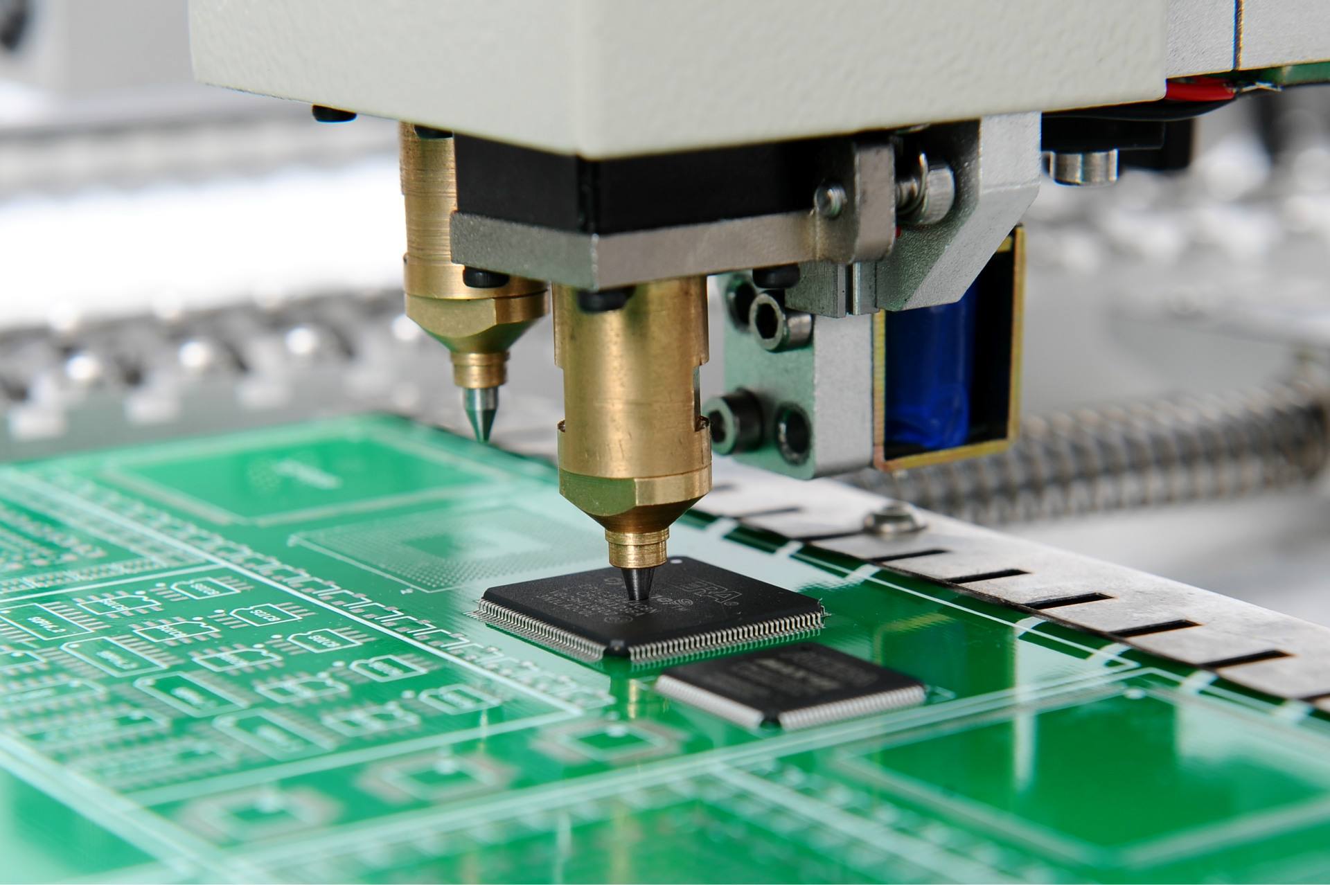
Design Guidelines for RF PCB Assembly RF PCBs can be manufactured in high yield by following some basic design guidelines required for RF PCB assembly. These rules are an extension of the standard DFM rules and will help in the manufacture of high output, high speed RF PCBs.
RF designs require higher power support. Therefore, thermal pads should be constructed for basic power needs and still be fabricated with the amount of heat dissipation required.
Placement of surface mount components must be considered in advance during the component placement phase. In RF designs, many metals are used for power networking and shielding purposes. These metal spaces should not be used by designers to place any SMT components.
The complex signal routing requirements of RF PCBs can lead to strict component placement strategies. But designers must consider necessary rework, debugging requirements during mass production, and must provide adequate space for component access.
Finding a middle ground that meets electrical requirements and manufacturability is possible if the designer carefully considers all design and assembly requirements for an RF PCB.
RF PCB Safe Handling Guidelines
The boom in wireless technology has ensured the need for high frequency RF PCBs in consumer products alongside traditional military or aerospace applications. The increasing number of RF-based products has resulted in a crowded RF spectrum and unwanted interference. Therefore, it is necessary to handle these RF PCB applications with caution.
Shielding the RF circuit board and its sensitive components can greatly reduce the threat of EMI interference. But this shielding can also interfere with the transmission of signals. Proper PCB grounding is very important in order to deal with EMI issues. Long, high-speed tracks can act as transmitters and receivers of electromagnetic interference. Therefore, adhering to the shortest possible trace length is important for any RF PCB design.
The design and manufacture of RF PCBs requires good domain knowledge and detailed PCB manufacturing experience. This comprehensive guide provides a combination of design, assembly, and safety factors to consider while designing an RF PCB. Don't forget to involve your PCB assembly supplier from the design stage to bring high performance RF PCBs to market.


Just upload Gerber files, BOM files and design files, and the KINGFORD team will provide a complete quotation within 24h.