
Professional PCB manufacturing and assembly
Building 6, Zone 3, Yuekang Road,Bao'an District, Shenzhen, China
+86-13410863085Mon.-Sat.08:00-20:00

SMT patch introduction
SMT patch refers to the abbreviation of a series of process processes processed on the basis of PCB. PCB (Printed Circuit Board) is a printed circuit board.
SMT is Surface Mount Technology (Surface Mount Technology) (abbreviation for Surface Mounted Technology), which is the most popular technology and process in the electronics assembly industry. Electronic circuit surface assembly technology (Surface Mount Technology, SMT), known as surface mount or surface mount technology. It is a kind of non-pin or short-lead surface mount components (SMC/SMD for short, Chinese called chip components) mounted on the surface of the printed circuit board (Printed Circuit Board, PCB) or the surface of other substrates, through Circuit assembly and connection technology that is soldered and assembled by methods such as reflow soldering or dip soldering.
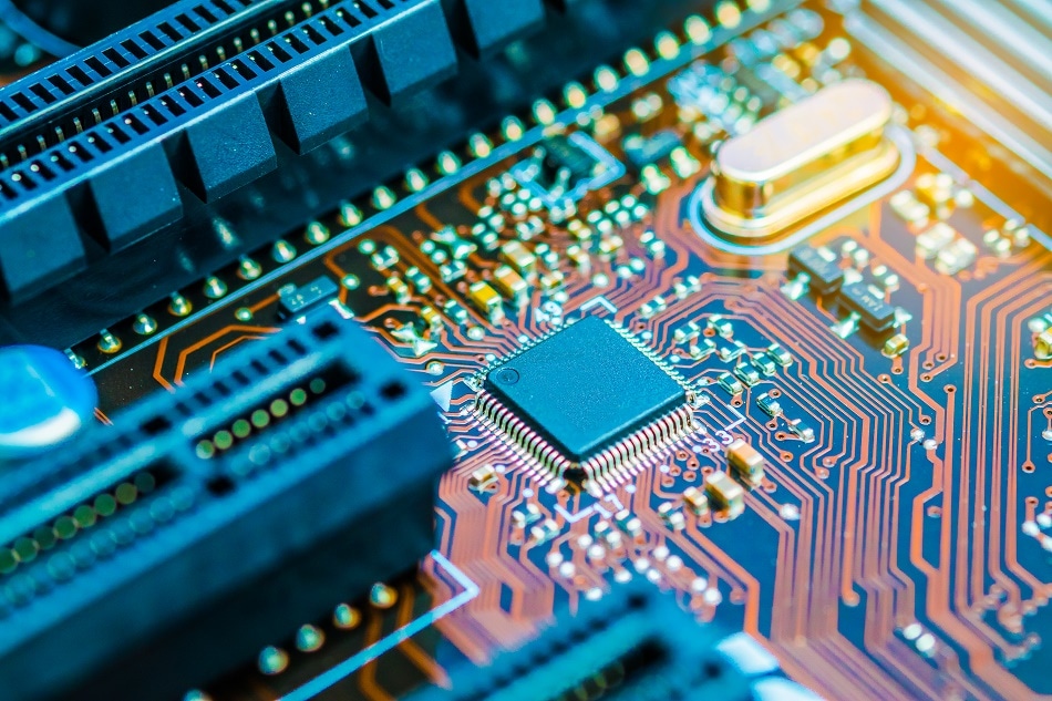
Under normal circumstances, the electronic products we use are designed by PCB plus various capacitors, resistors and other electronic components according to the designed circuit diagram, so all kinds of electrical appliances need a variety of SMT chip processing technology to process[ 1] .
SMT Basic Technology Broadcast
Solder paste printing --> parts mounting --> reflow soldering --> AOI optical inspection --> maintenance --> board separation.
Electronic products are pursuing miniaturization, and the perforated plug-in components used in the past can no longer be reduced. Electronic products have more complete functions, and the integrated circuits (IC) used have no perforated components, especially large-scale and highly integrated ICs, and surface mount components have to be used. Product mass production, production automation, the factory must produce high-quality products at low cost and high output to meet customer needs and strengthen market competitiveness. The development of electronic components, the development of integrated circuits (IC), and the multiple applications of semiconductor materials. The electronic technology revolution is imperative, and the pursuit of international trends. It is conceivable that when the production technology of international cpu and image processing device manufacturers such as intel and amd has improved to more than 20 nanometers, the development of surface assembly technology and technology such as smt is also unavoidable.
Advantages of smt patch processing: high assembly density, small size and light weight of electronic products, the volume and weight of patch components are only about 1/10 of traditional plug-in components, generally after using SMT, the volume of electronic products is reduced by 40%~60 %, the weight is reduced by 60%~80%. High reliability and strong anti-vibration ability. Solder joint defect rate is low. Good high frequency characteristics. Reduced electromagnetic and radio frequency interference. Easy to automate and improve production efficiency. Reduce costs by 30% to 50%. Save material, energy, equipment, manpower, time, etc.
It is precisely because of the complexity of the process of smt patch processing that there have been many smt patch processing factories specializing in smt patch processing. In Shenzhen, thanks to the vigorous development of the electronics industry, smt patch processing has achieved the prosperity of an industry.
Process broadcastSMT basic process components include: silk screen (or dispensing), placement (curing), reflow soldering, cleaning, testing, repair
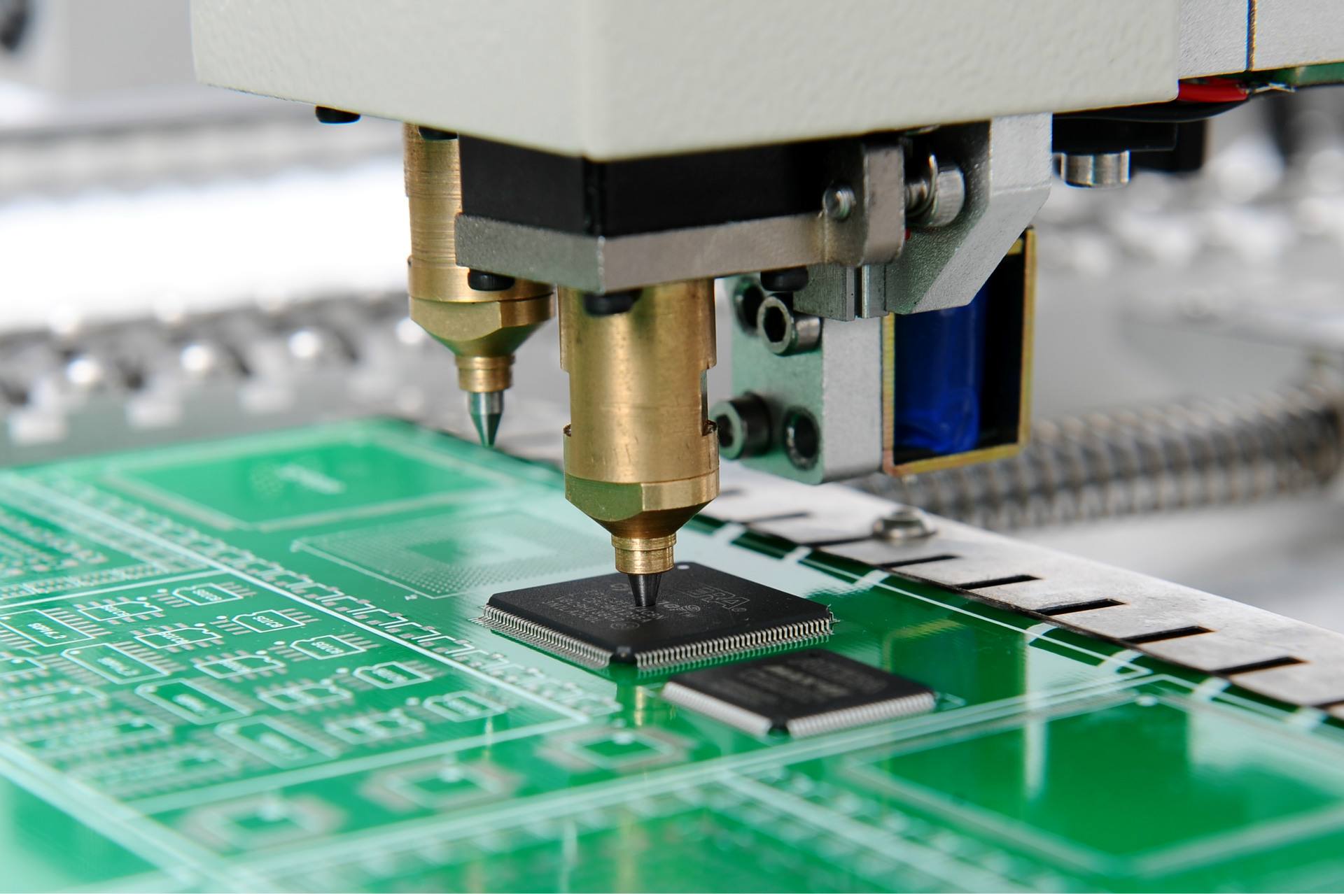
1. Silk screen printing: Its function is to leak solder paste or patch glue onto the pads of the PCB to prepare for the soldering of components. The equipment used is a screen printing machine (screen printing machine), which is located at the forefront of the SMT production line.
2. Glue dispensing: It is to drop glue onto the fixed position of the PCB board, and its main function is to fix the components to the PCB board. The equipment used is a glue dispenser, which is located at the forefront of the SMT production line or behind the testing equipment.
3. Mounting: Its function is to accurately install the surface mount components to the fixed position of the PCB. The equipment used is a placement machine, which is located behind the screen printing machine in the SMT production line.
4. Curing: Its function is to melt the adhesive, so that the surface mount components and the PCB board are firmly bonded together. The equipment used is a curing oven, which is located behind the placement machine in the SMT production line.
5. Reflow soldering: Its function is to melt the solder paste, so that the surface mount components and the PCB board are firmly bonded together. The equipment used is a reflow oven, which is located behind the placement machine in the SMT production line.
6. Cleaning: Its function is to remove the welding residues harmful to human body on the assembled PCB board, such as flux. The equipment used is a washing machine, and the location may not be fixed, online or offline.
7. Inspection: Its function is to inspect the welding quality and assembly quality of the assembled PCB board. The equipment used includes magnifying glass, microscope, online tester (ICT), flying probe tester, automatic optical inspection (AOI), X-RAY inspection system, functional tester, etc. The location can be configured in a suitable place on the production line according to the needs of detection.
8. Rework: Its function is to rework the PCB board that has failed. The tools used are soldering iron, rework station, etc. Configured anywhere in the production line.
SMT technology broadcast
Single-sided assembly
Incoming material inspection => silk screen solder paste (dot patch glue) => patch => drying (curing) => reflow soldering => cleaning => inspection => repair
double-sided assembly
A: Incoming material inspection => PCB A-side silk screen solder paste (dot patch glue) => SMD PCB B-side silk screen solder paste (dot SMT glue) => SMT => drying => reflow soldering ( Best only for side B => cleaning => testing => rework).
B: Incoming material inspection => PCB A-side silk screen solder paste (dot patch glue) => SMD => drying (curing) => A-side reflow soldering => cleaning => flipping = PCB B-side point SMD adhesive => SMD => Curing => B-side wave soldering => Cleaning => Inspection => Rework)
This process is suitable for reflow soldering on the A side of the PCB and wave soldering on the B side. In the SMD assembled on the B side of the PCB, this process should be used when only SOT or SOIC (28) pins are below.
Single side mixed process
Incoming material inspection => PCB A-side silk screen solder paste (dot patch adhesive) => patch => drying (curing) => reflow soldering => cleaning => plug-in => wave soldering => cleaning => inspection = > Repair
Double-sided mixed process
A: Incoming material inspection => SMT glue on the B side of the PCB => SMD => Curing => Flip board => Plug-in on the A side of the PCB => Wave soldering => Cleaning => Inspection => Rework
Paste first and insert later, suitable for the situation where there are more SMD components than discrete components
B: Incoming material inspection => PCB A-side plug-in (pins are bent) => flipping board => PCB B-side SMT glue => patch => curing => flipping board => wave soldering => cleaning => Inspection => Repair
Insert first and stick later, suitable for the situation where there are more separated components than SMD components
C: Incoming material inspection => silk screen solder paste on PCB side A => patch => drying => reflow soldering => plug-in, pin bending => flipping board => point adhesive on PCB side B => SMD => curing => flipping => wave soldering => cleaning => inspection => rework mixed assembly on side A and mounting on side B.
D: Incoming material inspection => SMT glue on the B side of the PCB => SMT => curing => flipping => silk screen printing solder paste on the A side of the PCB => SMT => A side reflow soldering => plug-in => B-side wave soldering => cleaning => inspection => rework A-side mixed assembly, B-side mounting. Paste SMD on both sides first, reflow soldering, then plug-in, wave soldering E: Incoming material inspection => PCB B-side silk screen solder paste (dot patch adhesive) => SMT => drying (curing) => reflow soldering = > Flip board => PCB A-side silk screen solder paste => patch => drying = reflow soldering 1 (local soldering can be used) => plug-in => wave soldering 2 (if there are few components inserted, manual soldering can be used) => Cleaning => Inspection => Rework A side mount, B side mixed.
Double-sided assembly process
A: Incoming material inspection, PCB A side silk screen solder paste (point patch adhesive), patch, drying (curing), A side reflow soldering, cleaning, flipping; PCB B side silk screen solder paste (point patch Glue), patch, drying, reflow soldering (preferably only for B side, cleaning, testing, rework)
This process is suitable for large SMDs such as PLCC mounted on both sides of the PCB.
B: Incoming material inspection, screen printing solder paste on the A side of the PCB (adhesive application), patching, drying (curing), reflow soldering on the A side, cleaning, and flipping; on the B side of the PCB, applying the SMT adhesive and patching , Curing, B-side wave soldering, cleaning, testing, rework) This process is suitable for reflow on the A-side of the PCB.
thin film printed circuit
Design to Handle RF PCBs
May 30,2023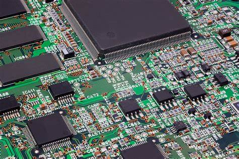


Just upload Gerber files, BOM files and design files, and the KINGFORD team will provide a complete quotation within 24h.