
Professional PCB manufacturing and assembly
Building 6, Zone 3, Yuekang Road,Bao'an District, Shenzhen, China
+86-13410863085Mon.-Sat.08:00-20:00

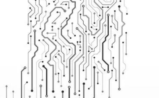
Differential Signal is used more and more widely in the design of high-speed circuits. The most critical signals in circuits often use differential structure. What is differential signal? In plain English, the driver sends two equivalent, inverting signals, and the receiver determines whether the logical state is "0" or "1" by comparing the difference between the two voltages. The pair carrying the differential signal is called differential routing.

Advantages of differential design routing:
Compared with ordinary single-ended signal routing, differential signal has the most obvious advantages in the following three aspects: a. Strong anti-interference ability because the coupling between two differential wires is very good, when there is noise interference from the outside, it is almost coupled to two lines at the same time, and the receiver only cares about the difference between the two signals, so the common mode noise from the outside can be completely cancelled out. b. Can effectively suppress EMI. Similarly, because the polarity of two signals is opposite, their electromagnetic fields can cancel each other. The closer the coupling, the less electromagnetic energy will be released to the outside world. c. Precise timing positioning Because the switching change of differential signal is located at the intersection of two signals, unlike ordinary single-ended signal which depends on high and low threshold voltage, it is less affected by technology and temperature, which can reduce the error in timing and is more suitable for the circuit with low amplitude signal. LVDS (low voltage differential signaling), which is popular at present, refers to this small amplitude differential signaling technology.
Points to note for differential design routing:
For PCB engineers, the most important thing is to ensure that the advantage of differential routing can be fully utilized in the actual routing. Perhaps as long as the contact with Layout people will understand the general requirements of differential routing, that is, "equal length, equal distance". The equal length is to ensure that the two differential signals maintain opposite polarity at all times and reduce the common-mode component. Equidistance is mainly to ensure that the difference impedance is the same, reduce reflection." As close to the principle as possible "is sometimes a requirement for differential routing.
Error of differential design routing:
1. It is believed that differential signals do not need ground plane as a return path, or that differential routes provide return paths for each other. The reason for this misunderstanding is that the surface phenomenon is confused, or the mechanism of high-speed signal transmission is not deep enough. In fact, in terms of signal reflux analysis, the mechanism of differential routing is the same as that of ordinary single-ended routing, that is, high-frequency signals always flow back along the loop with the smallest inductance. The biggest difference lies in that apart from the coupling to the ground, the difference lines also have coupling between each other. The strong coupling will become the main reflux path. In PCB circuit design, the coupling between differential routing is generally small, often accounting for only 10~20% of the coupling degree, more or the coupling to the ground, so the main return path of differential routing still exists in the ground plane.
Second, it is more important to maintain equal spacing than to match line length. In the actual PCB routing, the requirements of differential design can not be met at the same time. Due to the presence of pin distribution, hole crossing, wire space and other factors, it is necessary to achieve the purpose of line length matching through appropriate winding, but the result must be that part of the difference pair cannot be parallel.
At this time, how should we choose? From the perspective of theoretical analysis, although inconsistent spacing will lead to changes in differential impedance, the coupling between difference pairs itself is not significant, so the range of impedance changes is also small, usually within 10%, only equivalent to the reflection caused by a hole, which will not cause significant impact on signal transmission. Once the line length is not matched, in addition to the time sequence deviation, it also introduces common mode components into the differential signal, reducing the quality of the signal and increasing EMI. It can be said that the most important rule in PCB differential routing design is to match the length of the line, and other rules can be flexibly processed according to the design requirements and practical applications.
Three, think that the difference line must be very close. The purpose of having differential lines close together is to enhance their coupling, both to improve immunity to noise and to take full advantage of the opposing polarity of the magnetic field to counteract electromagnetic interference. Although this approach is very favorable in most cases, but not absolute, if we can ensure that they are fully shielded from external interference, then we do not need to achieve the purpose of anti-interference and EMI suppression through strong coupling with each other.
How to ensure that differential routing has good isolation and shielding? It is one of the most basic ways to increase the distance between the lines and other signals. The energy of electromagnetic field decreases with the square relationship between the distance. Generally, when the distance between the lines is more than 4 times the width of the lines, the interference between them will be extremely weak and basically can be ignored. In addition, isolation through the ground plane can also play a good shielding role.


Just upload Gerber files, BOM files and design files, and the KINGFORD team will provide a complete quotation within 24h.