
Professional PCB manufacturing and assembly
Building 6, Zone 3, Yuekang Road,Bao'an District, Shenzhen, China
+86-13410863085Mon.-Sat.08:00-20:00

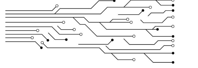
How to solve EMI problem in multi-layer PCB design
There are many ways to solve EMI problems. Modern EMI suppression methods include: using EMI suppression coating, choosing suitable EMI suppression parts and EMI simulation design. Starting from the most basic PCB board, this paper discusses the function and design skills of PCB stacking in controlling EMI radiation.
Power busbar
Reasonable placement of capacitors with appropriate capacity near the IC power supply pin can make the IC output voltage jump faster. However, the problem does not end there. Due to the finite frequency response nature of capacitors, this prevents them from generating the harmonic power needed to drive the IC output cleanly over the full frequency band. In addition, the transient voltage formed on the power busbar will form a voltage drop on the inductor ends of the decoupling path, and these transient voltages are the main common mode EMI interference sources. How do we solve these problems?
In the case of the IC on our circuit board, the power layer around the IC can be regarded as a good high-frequency capacitor, which can collect the energy leaked by discrete capacitors that provide high frequency energy for clean output. In addition, the inductance of a good power layer is small, so that the transient signal synthesized by the inductance is small, thus reducing common mode EMI.

Of course, the wiring from the power layer to the IC power supply pin must be as short as possible, because the digital signal is rising faster and faster, preferably directly to the pad where the IC power supply pin is located, which is discussed separately.
In order to control common-mode EMI, the power layer must be a reasonably well designed pair of power layers to facilitate decoupling and have sufficiently low inductance. One might ask, how good is good? The answer depends on the layering of the power supply, the materials between the layers, and the operating frequency (a function of the IC rise time). Typically, the power layers are 6mil apart and the interlayers are FR4, so the equivalent capacity per square inch of power layer is about 75pF. Obviously, the smaller the layer spacing, the larger the capacitance.
There are not many devices with rise times of 100 to 300ps, but at the current rate of IC development, there will be a high proportion of devices with rise times in the 100 to 300ps range. For circuits with 100 to 300ps rise times, 3mil layer spacing will no longer be appropriate for most applications. At that time, it is necessary to adopt the layering technique with layers less than 1mil apart and replace the FR4 dielectric material with a material with a very high dielectric constant. Today, ceramics and gattar plastics can meet the design requirements of 100 to 300ps rise time circuits.
Although new materials and methods may be used in the future, for today's common 1 to 3ns rise time circuits, 3 to 6mil layer spacing, and FR4 dielectric materials, it is generally sufficient to handle high end harmonics and keep the transient signal low enough, that is, common-mode EMI can be dropped very low. The PCB layer-stack design example presented in this paper will assume layer spacing of 3 to 6mil.
Electromagnetic shielding
From the point of view of signal wiring, a good layering strategy should be to place all signal wiring in one or more layers, which are next to the power layer or grounding layer. For power supplies, a good stratification strategy should be that the power layer is adjacent to the ground layer, and the distance between the power layer and the ground layer is as small as possible, which is what we call the "stratification" strategy.
PCB stacking
What stacking strategies help mask and suppress EMI? The following layered stacking scenario assumes that the power supply current flows across a single layer and that single or multiple voltages are distributed in different parts of the same layer. The case of multiple power layers is discussed later.
Four-ply plate
There are several potential problems with the 4-ply design. First of all, for the traditional four-layer plate with a thickness of 62mil, even though the signal layer is in the outer layer and the power supply and grounding layer are in the inner layer, the distance between the power supply layer and grounding layer is still too large.
If cost requirements are Paramount, consider the following two alternatives to traditional 4-ply panels. Both solutions can improve EMI suppression performance, but only when the density of the components on the board is low enough and there is sufficient area around the components to place the required power copper coating.


Just upload Gerber files, BOM files and design files, and the KINGFORD team will provide a complete quotation within 24h.