
Professional PCB manufacturing and assembly
Building 6, Zone 3, Yuekang Road,Bao'an District, Shenzhen, China
+86-13410863085Mon.-Sat.08:00-20:00

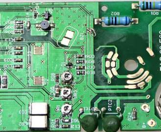
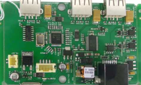
In the electronics industry,SMT patch processing is mainly processed by SMT, and there will be many failures in the process of use. According to statistics,60% of the defects are caused by solder paste printing. Therefore, it is an important premise to guarantee the printing quality of SMT patches. The following Kingford Xiaobian will introduce you to solve the printing error in the repair process.
1. There is no gap between the steel mesh and PCB printing mode, that is, "touch printing". The stability of various structures is required to be high, suitable for printing high precision solder paste. Metal plate and printed board good contact, after printing can be separated from PCB. Therefore, the method has a high printing precision, especially suitable for fine and ultrafine printing.
1. Printing speed.
The solder paste rolls forward when scraping the board. Suitable for screen printing fast printing.
This rebound, at the same time, can also prevent the solder paste from leaking, and the slurry in the net can not roll, resulting in clear solder paste, so printing too fast.
The scale is 10 x 20 mm/s.
2. Printing Method:
Contact or non-contact printing, screen printing and printed circuit board with blank printing method is "non-contact printing", generally 0.5×1.0mm, suitable for different viscosity solder paste. Push the solder paste into the steel mesh and press the PCB board with a scraper. After the scraper is removed, the steel mesh is isolated from the PCB board, thus reducing the risk of vacuum leakage to the steel mesh pollution.
3. Scraper type:
The scraper is divided into plastic scraper and steel scraper. For the IC with a distance of less than 0.5mm, steel solder paste can be used to form solder paste after printing.
4. Scraper adjustment.
During welding, the operating point of the scraper is printed in the direction of 45°, which can significantly improve the uneven opening and reduce the damage of the perforated sheet steel. The scraper pressure is usually 30N/mm.
Second, the installation should choose the IC installation height with the spacing not exceeding 0.5mm, 0mm or 0~ 0.1mm installation height, to avoid the welding paste falling off due to the installation height is too low, and the short circuit in the reflux.
Three, heavy fusion welding.
The main reasons for assembly failure caused by reflow welding are as follows:
First, the temperature is too fast;
b. high temperature and overheating;
The solder paste heating speed is faster than the circuit board heating speed;
d. Excess water.
Therefore, when determining the process parameters of refusion welding, all factors should be fully considered to ensure that there is no problem in welding quality before mass assembly.

2. Introduction to SMT lead-free welding and maintenance
The introduction of lead-free SMT patch assembly was always going to be a challenge for the first assembly, as it would be more challenging when machining and rework was needed. PCBA maintenance in a lead-free environment entails higher cost, quality detail, time, and repeatability issues -- all of which require attention due to lead-free requirements. Due to the need for lead-free process:
1. Train operators to perform lead-free assembly, maintenance and inspection, as well as assess time and cost.
2. Lead-free solder materials are higher than the traditional price, lead-free wire, electrode, wire core solder, etc.
3. The processing temperature of lead-free assembly (about 30-35℃) requires higher precision and precision.
4. Lead-free technology also requires research and planning of SMT factory to establish correct PCBA maintenance process.
It is considered that the best practice of PCB assembly rework should first be based on the characteristics of lead-free process, and the configuration file for technicians. To define the rework criteria, whether standard solder or lead-free solder is required, the process is the same - the steps required are:
1. Define and execute an accurate hot profile.
2. Remove the faulty component.
3. Clean the site of any rust or solder residue and prepare it for new components.
4. Replace parts with new solder and flux and reflow.
5. The rework has been thoroughly checked.
In lead-free environments, accurate and reliable rework is more difficult because PCbas and the parts closest to maintenance have to go through multiple high-temperature cycles, Genter said. In order to protect the stability of the circuit board, the preheating temperature should be set within the range of the glass transition temperature of the PCB material.
The subsequent steps involved in the rework process vary depending on lead-free requirements. The distinction between standard and lead-free presents many challenges that can only be addressed by the introduction of new or changing technologies, including more rigorous and accurate thermal curves and extremely high accuracy throughout the PCBA repair process. This avoids many costly problems caused by different heat distributions.


Just upload Gerber files, BOM files and design files, and the KINGFORD team will provide a complete quotation within 24h.