
Professional PCB manufacturing and assembly
Building 6, Zone 3, Yuekang Road,Bao'an District, Shenzhen, China
+86-13410863085Mon.-Sat.08:00-20:00


The laminated design of PCB is not a simple stacking of layers, in which the arrangement of layers is the key, and it has a close relationship with the arrangement and direction of signals. Compared with ordinary PCB, the design of multilayer board, in addition to adding the necessary signal routing layer, the most important thing is to arrange independent power supply and formation (copper layer). In high speed digital circuit systems, the advantages of using power and ground instead of the previous power and ground bus are:
1) Provide a stable reference voltage for digital signal transformation.
2) Evenly add power to each logic device at the same time.
3) Effectively inhibit crosstalk between signals.
The reason is that the use of a large area of copper as a power source and ground greatly reduces the resistance of the power source and ground, so that the voltage on the power layer is uniform and stable, and can ensure that each signal line has a very close to the ground plane, which also reduces the characteristic impedance of the signal line, and can effectively reduce crosstalk. Therefore, for some high-end high-speed circuit design, it has been clearly stipulated that we must use 6 layers (or more) of the laminated scheme, such as Intel's requirements for PC133 memory module PCB. This is mainly to take into account the electrical characteristics of the multilayer board, as well as the suppression of electromagnetic radiation, and even in the ability to resist physical and mechanical damage are significantly better than the number of low-level PCB.
In general, the laminated design is carried out according to the following principles: to meet the characteristic impedance requirements of the signal; Satisfy the minimization principle of signal loop; Meet the requirements of minimizing signal interference in PCB; It satisfies the symmetry principle. Specifically, the following aspects need to be paid attention to in the design of multilayer board:

1) A signal layer should be adjacent to a copper coating layer, and the signal layer and copper coating layer should be placed at intervals. It is best that each signal layer can be adjacent to at least one copper coating layer. The signal layer should be tightly coupled to the adjacent copper coating layer (i.e. the thickness of the medium between the signal layer and the adjacent copper coating layer is very small).
2) Power copper and ground copper should be tightly coupled and located in the middle of the lamination. Shortening the distance between the power supply and the formation is beneficial to the stability of the power supply and the reduction of EMI. Try to avoid the signal layer sandwiched between the power layer and the formation. The close proximity between the power plane and the ground plane is like forming a flat capacitor. The closer the two planes are, the larger the capacitor value. The main function of the capacitor is to provide a low impedance return path for high frequency noise (such as switching noise, etc.), so that the receiving device power input has a smaller ripple, enhance the performance of the receiving device itself.
3) At high speeds, excess layers can be added to isolate the signal layer. Multiple ground copper layers can effectively reduce the impedance of PCB and reduce common-mode EMI. But it is recommended not to add more power layer to isolate, which may cause unnecessary noise interference.
4) The high-speed signals in the system should be in the inner layer and between two copper compacts, so that the two copper compacts can provide shielding for these high-speed signals and limit the radiation of these signals to the two copper compacts.
5) Give priority to the transmission line model of high-speed signals and clock signals, design a complete reference plane for these signals, try to avoid cross-plane segmentation area, in order to control the characteristic impedance and ensure the integrity of signal return path.
6) When two signal layers are adjacent. For boards with high speed signals, the ideal lamination is to design a complete reference plane for each high speed signal layer, but in practice we always need to make a trade-off between the number of PCB layers and PCB cost. In this case, it is inevitable to have two signal layers adjacent to each other. The current approach is to increase the distance between the two signal layers and make the lines of the two layers as vertical as possible to avoid signal crosstalk between layers.
7) It is best to set the copper layer in pairs, such as the second, fifth or third and fourth layers of the six layers of the board together, which is to take into account the requirements of balanced structure in the process, because the unbalanced copper layer may lead to the warping deformation of PCB.
8) The secondary surface (i.e. the layer immediately adjacent to the surface) is designed as a stratum, which helps to reduce EMI.
9) Estimate the number of required signal layers according to PCB device density and pin density, and determine the total number of layers.
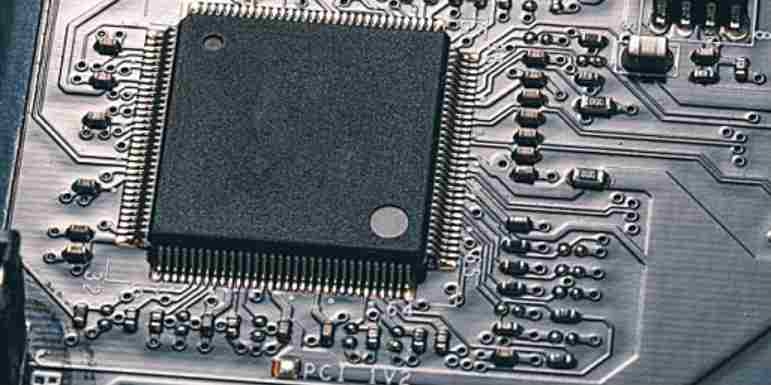
The structure of the board is a very important factor to determine the EMC performance of the system. A good board structure plays a good role in suppressing the radiation in PCB. In today's common high-speed circuit system, most of the use of multilayer panels rather than single and double panels. The following are four layers of board, six layers of board, eight layers of board, ten layers of board structure design to do a simple description.


Just upload Gerber files, BOM files and design files, and the KINGFORD team will provide a complete quotation within 24h.