
Professional PCB manufacturing and assembly
Building 6, Zone 3, Yuekang Road,Bao'an District, Shenzhen, China
+86-13410863085Mon.-Sat.08:00-20:00

A: The 2nd and 5th layers are power supply and ground copper coating. Due to the high impedance of power copper coating, it is very unfavorable to the control of common mode EMI radiation. However, from the point of view of impedance control of the signal, this method is very correct. Because in this kind of board design, Layer1 and Layer3, Layer4 and Layer6 of signal routing layer constitute two pairs of reasonable routing combination.
B: The power supply and the ground are placed in the 3rd and 4th layers respectively. This design solves the problem of copper impedance of the power supply. Due to the poor electromagnetic shielding performance of the 1st and 6th layers, differential mode EMI is increased. If the number of signal wires on the two outer layers is minimal and the line length is very short (less than 1/20 of the highest harmonic wavelength of the signal), then this design can solve the differential mode EMI problem. The non-component and non-wireline areas on the outer layer are filled with copper and the copper area is grounded (at intervals of 1/20 wavelength), so the suppression of differential mode EMI is particularly good.
C: From the point of view of signal quality, it is obvious that this arrangement is the most reasonable. Because such a structure is ideal for the high frequency return path of the signal. However, this arrangement has a more prominent disadvantage, that is, the signal line layer is less. So such a system is suitable for high performance requirements.

D: This can achieve the required environment for signal integrity design. The signal layer is adjacent to the grounding layer, and the power layer is paired with the grounding layer. Obviously, the disadvantage is that the structure of the layers is not balanced (an unbalanced copper coating may cause the PCB to warp and deform). The solution to the problem is to apply copper to all the blank areas of the third layer. After applying copper, if the copper density of the third layer is close to that of the power layer or ground layer, this board can be loosely counted as a structurally balanced circuit board. The copper area must be connected to the power supply or grounded.
Eight-layer board design
Table 3 Example of eight-layer lamination
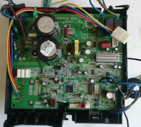
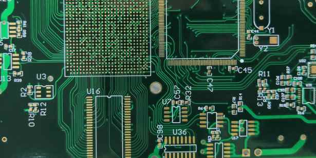
PCB laminated design
Most of the eight-layer plates in use are designed to improve the signal quality of six-layer plates. As can be seen from Table 3, compared with six-layer board, eight-layer board does not add signal routing layer, but two more copper coating layers, so the EMC performance of the system can be optimized.
Ten layer board design
Table 4 Examples of ten laminated panels
PCB laminated design
The 10-layer PCB insulating dielectric layer is very thin, and the signal layer can be very close to the ground plane, so the impedance change between the layers is very well controlled. Generally, as long as there is no serious laminated design error, designers can easily complete high-quality high-speed circuit board design. If the wiring is very complicated and requires more wiring layers, we can set the layering as: Signal - Signal - Ground - signal - signal - signal - signal - signal - signal - power - signal - signal. Of course, this situation is not optimal. We require signal routing to be completed in a small number of layers, but use excess layers to isolate other signal layers, so the more common lamination scheme is: signal - ground - signal - signal power - ground - signal - signal - signal - signal - signal. As you can see, three floor layers are used and only one power layer is used (we only consider the case of a single power supply). This is because, although the effect of the power layer on the impedance control is the same as that of the ground plane layer, the voltage on the power layer is more disturbed, there are more high order harmonics, and EMI is strong to the outside world, so it is the best to be shielded by the ground plane, like the signal routing layer. At the same time, if the excess power layer is used for isolation, the loop current will have to be converted from the ground plane to the power plane by decoupling capacitors. Thus, too much voltage drop on the decoupling capacitor will produce unnecessary noise.
In fact, the above principles need to be applied flexibly in the laminated design. Sometimes not all principles can be met at the same time or all principles can be applied optimally, so it is necessary to select and determine the appropriate board structure based on the actual system requirements.


Just upload Gerber files, BOM files and design files, and the KINGFORD team will provide a complete quotation within 24h.