
Professional PCB manufacturing and assembly
Building 6, Zone 3, Yuekang Road,Bao'an District, Shenzhen, China
+86-13410863085Mon.-Sat.08:00-20:00

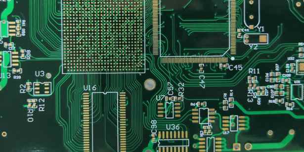
In PCB board backwelding furnace prone to plate bending and plate warping, we all know, so how to prevent PCB board backwelding furnace plate bending and plate warping, the following for you to elaborate:
1. Reduce the influence of temperature on the stress of PCB board
Since "temperature" is the main source of plate stress, so as long as reducing the temperature of the backwelding furnace or slow down the heating and cooling speed of the plate in the backwelding furnace, the bending and warping of the plate can be greatly reduced. But there may be other side effects, such as a short circuit in the solder.
2. High Tg plate is used
Tg is the glass conversion temperature, that is, the temperature at which the material changes from glass state to rubber state. The lower the Tg value is, the faster the board will become soft after entering the backwelding furnace, and the longer it will take to become soft rubber state, the more serious the deformation of the board will be. The circuit board with higher Tg plate can increase its ability to withstand stress and deformation, but the price of the material is relatively high.
3. Increase the thickness of the circuit board
Many electronic products in order to achieve the purpose of thinner, the thickness of the board has been left 1.0mm, 0.8mm, and even 0.6mm thickness, such a thickness to keep the board after the welding furnace without deformation, really a bit of a force, it is suggested that if there is no light and thin requirements, the board can use the thickness of 1.6mm, Can greatly reduce the risk of bending and deformation of the plate.
4. Reduce the size of the circuit board and reduce the number of boards
Since most backwelding furnaces use chains to drive the circuit board forward, the larger the size of the circuit board will sag and deform in the backwelding furnace because of its own weight, so try to put the long side of the circuit board as the board side on the chain of the backwelding furnace, you can reduce the weight of the circuit board caused by the sag deformation, reduce the number of plates is also based on this reason, That is to say, when the furnace, try to use the narrow side of the vertical direction of the furnace, can reach the lowest depression deformation.
5. The tray fixture has been used
If the above methods are difficult to achieve, * is to use reflow carrier/template to reduce the deformation. The reason why the plate bending and warping can be reduced by using the Reflow carrier/template is that the tray is expected to hold the circuit board no matter it is hot expansion or cold contraction. After the temperature of the circuit board is lower than Tg value and begins to harden again, It can also maintain the size of the garden.

If a single layer of tray can not reduce the deformation of the circuit board, it is necessary to add a layer of cover, the circuit board with two layers of tray clip up, so that you can greatly reduce the circuit board over the welding furnace deformation problem. But the trays are expensive, and you have to add labor to place and retrieve them.
6. Use the Router instead of the V-Cut
Since V-cuts can damage the structural strength of the board, try not to use V-Cut subboards, or reduce the depth of the V-Cut.
Preweight and deweight: This technique predistorts the signal before it is sent so that the quality of the signal on the receiver is the same as the quality of the original transmission. When the signal is held at the DC level for longer than one bit, the pre-weighting raises the high frequency component and lowers the low frequency component. In the process of designing these methods, the system designer must carefully control the output amplitude to limit the output power.
Receive equalization: Receive equalization compensates for channel loss characteristics by applying relative frequency characteristics to input data. There are two kinds of equalization circuits: stationary and adaptive. The fixed equalizer sets the compensation features manually, while the adaptive equalizer uses an adaptive algorithm to set the best compensation features, which enables the user to apply one device to various channels. It can also automatically compensate for changes in channel characteristics caused by manufacturing deviations and environmental changes.
The receive balancing function can be integrated into the backplane interface components or implemented in independent components. The advantage of performing reception equalization in standalone devices is that it provides optimal wiring advantage and design flexibility.
Crosstalk noise cancellation: In addition to pre-weighting and receiving equalization techniques, crosstalk cancellation is also used in some systems. These chips employ a noise cancellation mechanism that samples noise on adjacent channels and subtracts it from the signal.


Just upload Gerber files, BOM files and design files, and the KINGFORD team will provide a complete quotation within 24h.