
Professional PCB manufacturing and assembly
Building 6, Zone 3, Yuekang Road,Bao'an District, Shenzhen, China
+86-13410863085Mon.-Sat.08:00-20:00

In PCB design, wiring is an important step to complete the product design, it can be said that the previous preparation work is done for it. PCB routing includes single - sided routing, double - sided routing and multi - layer routing. Wiring mode also has automatic wiring and interactive wiring two kinds. Today, let the professional engineer for you detailed PCB wiring rules and skills are what?
1. Processing of power supply and ground wire
Interference caused by improper handling of power supply and ground wire will degrade the performance of products, and sometimes even affect the success rate of products. So the wiring of the power supply and ground wire should be taken seriously, the noise interference generated by the power supply and ground wire should be reduced to a minimum to ensure the quality of the product. Specific practices are as follows:
(1) Add decoupling capacitance between the power supply and ground wire.
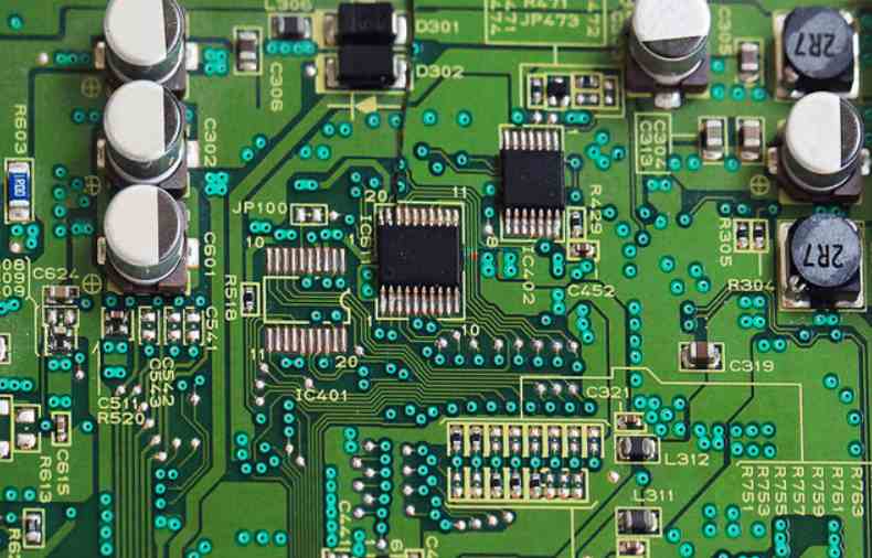
(2) Try to widen the width of the power supply and ground wire. The relationship between them is ground wire > power cable > signal cable. Usually, the width of signal wire is 0.2 ~ 0.3mm, the maximum width can reach 0.05 ~ 0.07mm, and the power cable is 1.2 ~ 2.5mm.
(3) The PCB of the digital circuit can be composed of a wide ground wire to use a loop.
(4) Made of multi-layer board, power supply, ground wire occupy a layer.
2. Common ground processing of digital circuit and analog circuit
There are many PCBS that are not single-function circuits, but consist of a mixture of digital and analog circuits. Therefore, it is necessary to consider the interference between them when wiring, especially the noise interference on the ground wire.
The frequency of digital circuit is high, and the sensitivity of analog circuit is strong. For ground wire, PCB has only one node to the outside world, so the problem of number and mode common ground must be dealt with inside PCB. The digital ground and the analog ground are actually separated inside the board, only in the PCB and the outside connection interface (such as plug, etc.), the digital ground and the analog ground only one connection point.
3. The signal cable is distributed on the electrical (ground) layer
In the multi-layer printed board wiring, because in the signal line layer is not finished and space is not much, more layers will cause waste. To solve this contradiction, wiring can be considered at the electrical (ground) level. The power layer should be considered first and the formation second.
4. Processing of connecting legs in large area conductors
In ground (electric) of large area, the legs of common components are connected with it. As far as electrical performance is concerned, it is good for the welding pad of the component leg to be fully connected with the copper surface, but there are some hidden dangers in the welding assembly of the component: (1) welding requires a high-power heater; (2) easy to cause virtual solder joint. So taking into account the electrical performance and process needs, made into a cross welding pad, commonly known as hot welding pad. In this way, the possibility of virtual welding spot caused by excessive heat dissipation in the welding section is greatly reduced.
5. The role of network system in wiring
In many CAD systems, the wiring is determined by the network system. The grid is too dense, although the path is increased, the storage space of the equipment must have higher requirements, but also has a great impact on the computing speed of electronic products. Too sparse grid and too few channels have great influence on the propagation rate. Therefore, it is necessary to have a reasonably dense grid system to support the wiring.
6. Design Rule Check (DRC)
After the wiring design is completed, it is necessary to carefully check whether the wiring design is reasonable. The general check includes the following aspects:
(1) Whether the distance between wire and wire, wire and component pad, wire and through hole, component pad and through hole, through hole and through hole is reasonable?
(2) Whether the width of the power cord and ground wire is appropriate? Is the power supply tightly coupled to the ground? Is there any place in the PCB where the ground wire can be widened?
(3) Whether the analog circuit and the digital circuit have their own ground lines?
(4) Will the graphics (such as ICONS and marking) added to the PCB later cause signal short circuit?
(5) Is there a process line on the PCB board? Does solder resistance meet the requirements of the production process? Is the solder resistance size appropriate? Are character marks pressed on device pads, etc.
Selective welding of printed circuit board
Mar 17,2023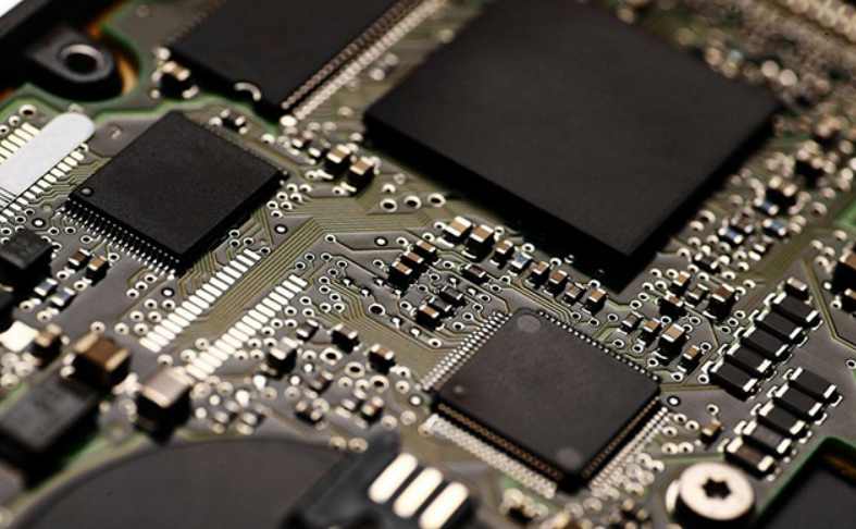


Just upload Gerber files, BOM files and design files, and the KINGFORD team will provide a complete quotation within 24h.