
Professional PCB manufacturing and assembly
Building 6, Zone 3, Yuekang Road,Bao'an District, Shenzhen, China
+86-13410863085Mon.-Sat.08:00-20:00

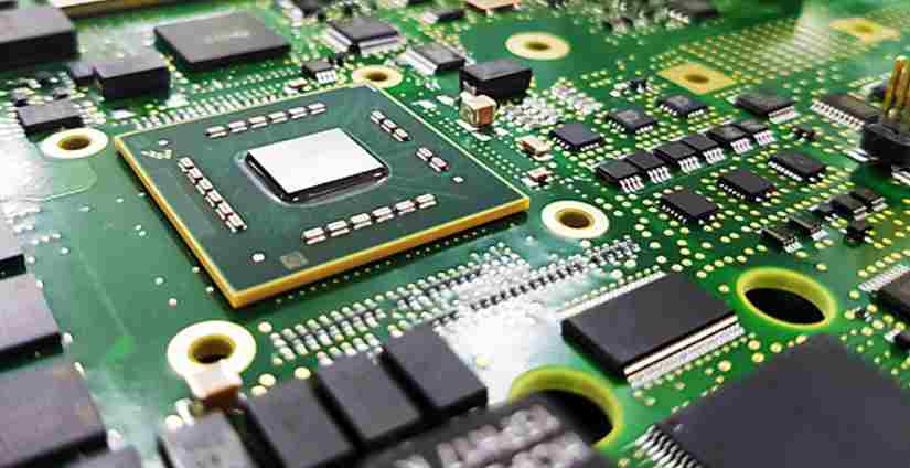
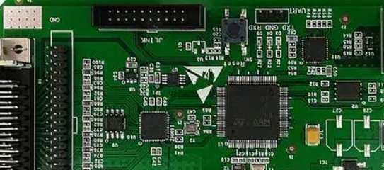
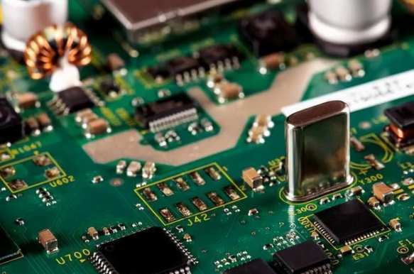
Bulk material of SMT patches refers to the parts that are separated from the original packaging during the production process due to the machine throwing or assembling and disassembling materials. No matter in the order of SMT patch factory's own contract of work and materials or the order of customer's supply of materials, the quantity of many class A materials is just right. Therefore, in the process of order clearance, bulk materials must be rearranged and pasted on PCBA surface. Some bulk materials, such as capacitors, resistors, inductors and other devices, due to their small value, and no reuse value, this kind of can be ignored, but there are some imported chip components, high value and easy to distinguish, so this kind of general to reuse. Therefore, we need to have a correct method of handling bulk materials. Strengthen the control of SMT bulk material to prevent the bad operation caused by the loading of bulk material. Next, SMT patch processing manufacturer -kingford- will share with you how to deal with SMT patch bulk material.
I. Responsibilities of SMT positions for bulk material cleaning
Operator: Responsible for the collection, classification, identification, storage, Posting and Posting information transfer of SMT patch tail cleaning bulk materials. Pre-furnace QC: Be responsible for SMT patch cleaning bulk material manual mounting, pre-mounting back grain and material code confirmation, PCBA identification mark. Line leader: responsible for supervising operators to complete the work according to the process and managing bulk materials. Inspector: Responsible for confirming and inspecting the first part of bulk material and checking the status of PCBA mark.
Second, SMT patch tail cleaning bulk material specific work content
1. Loose material may be produced by throwing material due to equipment and other factors during SMT placement. Therefore, during the operation, the operator should check the material spacing before SMT placement and during shift shift, check the throwing box and trash can every time garbage is poured, collect loose material, and report excessive abnormal bulk material to the line length.
2. Classify the bulk materials according to the appearance of the components, check the back grain of the components to determine the material code, and then pack the checked bulk materials in anti-static bulk boxes or bulk bags, and make the material code label, and sign the relevant confirmators.
3. First collect a certain length of used braid and one, and then use double-sided tape to stick the braid to the position where the patch function can absorb the material normally. It is best to ensure that the position of the material slot is aligned. Then prepare a program that can use the tray, so that the machine can be installed effectively, quickly and accurately.
4. For manually pasted materials, the operator needs to make a mark on the laminator to make the state clear in front of the furnace, and check the prototype when the QC starts to paste the first piece of bulk material in front of the furnace.
In addition, in SMT patch processing, normal incoming materials are generally based on the material plate as the carrier, and small-batch orders are generally based on the material belt packaging as the carrier, while bulk materials are different. Bulk materials cannot be machined directly without the material belt as the carrier. As for bulk materials, SMT SMT manufacturers need to finish them manually before SMT SMT starts. This part will cost a lot of labor costs, which is unfavorable to the overall SMT operating cost, and will delay more production efficiency and even lead to delayed delivery. Many SMT patch manufacturers will charge labor fees for orders with more serious bulk materials.

2. Clean free process in PCBA processing
Clean free refers to the process technology of using low solid content and non-corrosive flux in PCBA processing, welding under inert gas environment, after welding, the residues on the circuit board have no corrosion and have very high surface insulation resistance, and can reach the standard of ion cleanliness without cleaning under normal circumstances, and can directly enter the next PCBA processing process.
First, the advantages of PCBA processing without cleaning technology
1, a large amount of saving cleaning labor, equipment, sites, materials (water, solvent) and energy consumption; 2. Save working hours and improve production efficiency; 3, advanced production technology: spray coating, inert gas protection; 4, avoid cleaning stress damage to welding components; 5, conducive to environmental protection;
Two, PCBA processing without cleaning material requirements
1, low solid content: the requirement is less than 2%, solid content of traditional flux: 5% ~ 40% without rosin;
2, non-corrosive, high surface insulation resistance, not allowed to contain halogen components, high insulation resistance: 1.0X10^11;
3, weldability requirements: insoluble acetic acid series has a certain ability to eliminate oxides and maintain a certain degree of activity.
4, meet the requirements of environmental protection: non-toxic, no strong irritating smell, basically does not pollute the environment, safe operation.
In the process of PCBA welding without cleaning, the weldability and cleanliness of PCB and its components need to be controlled. In order to ensure the weldability, under the premise that the supplier is required to guarantee the weldability, the PCBA processing manufacturer shall store it in a constant temperature and dry environment, and strictly control the use of it within the effective storage time. In order to ensure cleanliness, PCBA processing process to strictly control the environment and operation specifications, to avoid man-made pollution, such as handwriting, sweat, grease, dust, etc.
3. PCBA process without cleaning
1. Coating process of flux: In order to obtain better cleaning free effect during PCBA processing, two parameters must be strictly controlled during flux coating process, namely solid content of flux and coating amount.
2. Spray coating:
(1) Due to the high solvent content of no-cleaning flux, it is particularly easy to volatilize, which leads to the increase of solid content. Therefore, spray method can effectively solve the problem of flux volatilization.
(2) Because the solid content of no-cleaning flux is very low, it is not conducive to foaming coating.
③, spray method can control the amount of flux coating, coating is uniform.
(4) Flux spray system adopts scanning spray mode, and adopts limit proximity switch and light eye to combine control. PCBA plate automatic detection and induction spray is carried out according to the speed and width of PCBA. Make the flux wetting range to achieve the best effect, imported nozzle and rod cylinder, special drive control system, accurate and reliable.
⑤, equipped with adjustable direction, air pressure knife, will spray the excess flux blown into the recycling box, prevent flux into the preheating area, to ensure production safety;
⑥, in the use of spray coating process must pay attention to one point, because the flux contains more flammable solvent, spray solvent vapor has a certain risk of deexplosion, so the PCBA processing equipment needs to have good exhaust facilities and necessary fire extinguishing equipment.
The above content is provided by PCBA processing manufacturer-kingford- for you. To learn more about PCBA processing knowledge, please visit the official website of Shenzhen One Nine Four Two Technology Co., LTD


Just upload Gerber files, BOM files and design files, and the KINGFORD team will provide a complete quotation within 24h.