
Professional PCB manufacturing and assembly
Building 6, Zone 3, Yuekang Road,Bao'an District, Shenzhen, China
+86-13410863085Mon.-Sat.08:00-20:00

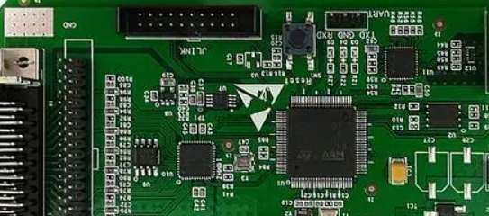
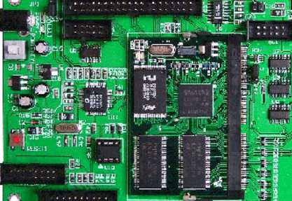
SMT processing mainly involves raw materials including PCB, solder paste and electronic components. The function of solder paste is to form an electrical and mechanical connection between PCB and electronic components through reflow welding, and PCB is the carrier of solder paste and electronic components. Therefore, the pass-through rate affecting PCBA processing and welding mainly depends on PCB in the SMT process. If PCB can be stored and inspected effectively and properly, welding defects can be reduced and SMT pass rate can be improved. Next, Shenzhen SMT manufacturer -kingford- will share the PCB storage and inspection specifications of SMT factory for you. Hope to bring you some help!
I. PCB inspection standard and inspection content
1. Inspection standards
① Inspection standards for R & D department or engineering department formally issued the sample acceptance letter shall be subject to.
(2) The appearance inspection items recorded in the sample recognition book should be included in the appearance management items for inspection. When necessary, limit samples can be set to manage, but when customers have special requirements, the acceptance standards for appearance inspection should be recognized by customers.
③ The sampling scheme shall be determined according to the sampling standard of SMT factory. In principle, sampling inspection should be carried out according to the number of inspections, or all inspections may be carried out. If there are special requirements, inspections should be carried out according to special requirements.
④ All incoming materials must be vacuum packed. If the vacuum package is unpacked during the inspection, it should be vacuum packed again within 2 hours after the inspection, and the corresponding information such as model, code and production cycle should be marked. After passing the inspection, the outer box shall be stamped with a qualified seal.
2. Check the content
① Appearance inspection: PCB board in the factory before the general experience of Electrical Test (Electrical Test), we receive by visual inspection inspection PCB board appearance items including warping, scratching, flying line, broken line, ink plugging, screen printing is not clear, pad oxidation, pad uneven, through the hole, plate edge burr;
② Size measurement: Use micrometer to measure whether the thickness, shape, size and V-CUT of PCB board conform to the design of Gerber file.
③ Furnace temperature test: many PCB board due to poor process control, so that PCB board after reflow welding and other high temperature phenomenon occurs yellow, warped. In the early stage of SMT processing, it is necessary to require the PCB board to pass the furnace temperature test first, so as to avoid bad welding or affect the future reliability and durability of the product.

④ Pad welding force test: the surface treatment process of many PCB board factories is generally exported, which makes the control ability of this process is very poor. Surface treatment is very important for SMT welding. Therefore, it is necessary to select a small sample of PCB bare board to brush solder paste and simple patch, so as to test the welding performance of components.
⑤ Check PCB board factory report: PCB board factory will generally send PCB slices and factory report with the goods. This report will elaborate on the production process of PCB board, the through-through rate in the process and the state of slice, etc. If individual abnormal items are found, project review shall be carried out in time.
2. Storage requirements
1, temperature: 26℃±3. Humidity: In an environment with non-corrosive gas less than 70%RH, if the humidity is too high, take proper ventilation and dehumidification measures.
2. When PCB is stored in the warehouse, the height of PCB outer box can not exceed 1 meter, and the outer box must overlap with each other to prevent tilt and collapse when stacked. When stacking, it is required to face outward with labels for easy viewing. Those with special requirements shall be dealt with according to their requirements.
3. The remaining unsealed printed boards shall be vacuum-packed within 4 hours after the warehouse sends the materials. During vacuum packing, the packing quantity of each bag shall be carried out according to the requirements in Table 1:
4. Effective storage period of PCB is 8-12 months (subject to PCB production date). The storage time of OSP PCB is 6 months.
5. After the storage period is exceeded, the valid storage period of PCB shall be 3 months (subject to the IQC inspection date). When the OSP PCB exceeds the storage period, please ask the supplier to assist in heavy processing. During heavy processing, it is necessary to slice and measure the copper thickness, measure the film thickness and conduct solder test. After passing the test, the PCB can continue to be used; otherwise, it can be disposed of completely. Where there are special requirements in the letter of recognition, such special requirements shall be followed.
6. Strictly control the storage time of PCB in the warehouse according to the principle of first in first out when distributing materials. For the same PCB from different suppliers, the principle of first in first out should also be followed, but the different suppliers and their quantity must be indicated on the corresponding material distribution sheet.
Three, use requirements
1. Do not directly touch the PCB board with your hands. Wear gloves when taking the PCB to prevent the printed board from being polluted by sweat or oil stains. Hand-held plate edge, do not touch the surface of the pad, to prevent the pad surface scratches, scrapes and pollution; Especially chemical nickel gold and OSP plate. In the process of taking the board and operation should be handled lightly; PCBS cannot be rubbed against each other to avoid mechanical damage to the printed board surface.
2. The packaged printed board can be transported by any method, but it should be protected from sun, rain, moisture, heat, mechanical damage and heavy pile pressure during transportation.
3. When PCB is stored in SMT process, long-term high temperature and uneven force extrusion must be prevented to prevent PCB deformation and distortion.
4. Check before unpacking. PCB is not allowed to have obvious appearance defects such as vacuum packing damage, over-storage period, scratches, bubbles, and pad oxidation.
5. Bake the damaged vacuum-packed PCB before going online according to the specific conditions (except OSP board, silver board, chemical nickel gold and non-welded mother board).
6. No matter whether the vacuum packaging is intact or not, PCB that has passed the inspection during the super storage period must be treated with drying board (except OSP board) before going online. During production, the engineering and quality department should be informed to check the welding status on site and confirm the welding quality.
The above content is provided by SMT factory kingford. For more knowledge about PCB board welding, please visit the official website of Shenzhen kingford Co., LTD
How to deal with SMT patch bulk material?
Mar 17,2023


Just upload Gerber files, BOM files and design files, and the KINGFORD team will provide a complete quotation within 24h.