
Professional PCB manufacturing and assembly
Building 6, Zone 3, Yuekang Road,Bao'an District, Shenzhen, China
+86-13410863085Mon.-Sat.08:00-20:00

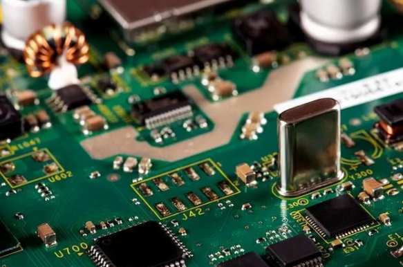
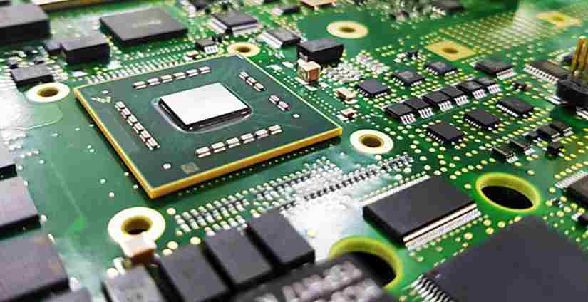
PCBA machining welding, there will be a lot of technology applications. The application of technology brings about the requirements for PCB board. If there are problems with PCB board, it will increase the difficulty of processing and welding process, which may eventually lead to welding defects. Therefore, only through a reasonable specification of the design of PCB board, in order to give full play to the processing capacity of the equipment, improve production efficiency and product quality. In order to ensure the quality of patch processing and welding, kingford sorted out some process requirements for PCB board during PCBA processing and welding and shared them with you. Hope to bring you some help!
1. Heat resistance
With the development of PCBA processing technology and the requirements of environmental protection, lead-free process has been widely used. At the same time, lead-free process has higher welding temperature, so it puts forward higher requirements on the heat resistance of PCB. During reflow welding, the temperature of lead-free process should reach 217~245℃ and the time lasts 30~65s. Generally, the heat resistance of PCB board should reach 260 degrees Celsius, and keep the requirement of 10s.
2. PCB appearance
PCB is generally rectangular, and the best aspect ratio is 3:2 or 4:3. When the ratio of length to width is large, it is easy to produce warping deformation. It is suggested to standardize PCB size as far as possible, which can simplify the processing process and reduce the processing cost.
3. PCB size
Different SMT equipment has different requirements on PCB size. In the early stage of PCB design, it is necessary to consider the maximum and minimum PCB mounting size of processing equipment. The general size is 50×50mm~400×460mm.
5. PCB process edge
In the process of PCBA processing, it is completed by rail transmission. In order to ensure that PCB is reliably fixed, 5mm is generally reserved on the side of the transmission track (long side) for the convenience of equipment clamping. It is not allowed to mount devices within this range. If no reservation can be made, the process edge must be added. For some plug-in wave-soldering products, the general side (short side) needs to be reserved for 3mm in order to block tin.
6. PCB benchmark identification points
The benchmark identification point, also known as Mark, provides a common reference point for all steps in the SMT assembly process, ensuring that each device used in the assembly can accurately locate the circuit pattern. Therefore, Mark point is very important for PCBA processing. Mark point is generally divided into the whole plate Mark, plate Mark, local identification Mark(foot spacing ≤0.5mm), generally specified Mark point center mark point for metal copper foil, 1.0mm in diameter, surrounding open contrast area diameter 3mm, metal copper foil and surrounding open area color contrast should be obvious. Screen printing, pad or V-Cut are not allowed within Φ3mm.
7. Block design
General principle: When PCB board size < 50mm×50mm, must do the plate. So that it can be converted to meet the production requirements of the ideal size, for plug-in and welding, improve production efficiency and equipment utilization. But pay attention to the size of the plate is not too large, and to meet the requirements of PCBA processing equipment. V-shaped slots, stamp holes or punching slots can be used between the plates;
8, can withstand solvent washing
In the process of PCBA processing, the solder joint is easy to get dirty due to the presence of flux in the solder paste, and it often needs to be cleaned with solvents such as plate washing water. So PCB should be able to withstand solvent washing, PCBA surface can not appear bubbles and white - some undesirable phenomena

2.SMT patch defective repair skills and process requirements
In our common SMT patch processing process, there will be more or less bad welding phenomena after reflow welding. Therefore, it is necessary for us to manually use tools to repair, so as to obtain qualified PCBA solder joints. Next, I will share with you the SMT patch repair skills and requirements, hope to bring you some help!
First, repair skills
1. During manual repair and welding, the SMT patch components should be welded according to the principle of small before large, low before high. First, chip resistance and chip capacitor transistor should be welded, and then small IC devices and large IC devices should be welded.
2. When welding chip components, the width of the selected soldering iron head should be consistent with the width of the components. If it is too small, it is not easy to locate when installing welding.
3. When welding devices with pins on both sides or four sides such as SOP, QFP, PLCC, etc., several anchor points should be welded on both sides or four sides first. After careful inspection to confirm that each pin is consistent with the corresponding pad, drag welding can be performed to complete the welding of the remaining pins.
4, drag welding speed is not too fast, IC about 1s drag 1-2 solder joints can be.
5, after welding can be used 4~6 times the magnifying glass to check whether there is a bridge between the welding spot, the same part of the continuous welding not more than two times. If it is not well welded, it should be welded after cooling to prevent the pad from falling off.
6. When welding IC devices, evenly coated with a layer of welding aid paste on the pad, it can not only play the role of infiltration and welding aid on the solder joint, but also improve the maintenance efficiency.
Two, repair process requirements
1, the operator should bring anti-static bracelet, generally requires the use of anti-static constant temperature electric iron, the use of ordinary electric iron must be well grounded.
2. Small power electric soldering iron of 15 ~ 20W should be used when repairing chip components. The temperature of the iron head should be controlled below 250℃.
3. The welding time should not be too long, otherwise it is easy to burn the components. The welding time of chip components should not exceed 5 seconds, and the welding times of the same welding spot should not exceed two times.
4, the solder joint should be a sine wave peak shape, the surface should be bright and smooth, Wuxi thorn, moderate tin.
5. After welding, the residual flux on the circuit board should be cleaned with alcohol to prevent the flux after carbonization from affecting the normal operation of the circuit.
6. When removing components for SMT patch repair, the components should be removed when the solder is completely melted, in order to avoid damaging the coplane of the pin of the device.
The above content is provided by Shenzhen kingford. To learn more about SMT, please visit the official website of Shenzhen kingford Co., LTD


Just upload Gerber files, BOM files and design files, and the KINGFORD team will provide a complete quotation within 24h.