
Professional PCB manufacturing and assembly
Building 6, Zone 3, Yuekang Road,Bao'an District, Shenzhen, China
+86-13410863085Mon.-Sat.08:00-20:00

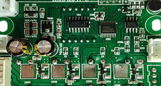
Solder pad is the basic unit of PCB surface mounting assembly. On the printed circuit board, the circuit connection of all components is carried out through the pad. Next, Shenzhen PCB design company - Shenzhen kingford to introduce the common PCB design pad shape and size standards.
First, PCB design of the common pad shape
Welding pad can be divided into 7 categories, according to the shape of the distinction is as follows:
1. Square pad - printed board components are large but few, and printed wire is simple.
2. Round pad - widely used in single and double sided printed boards with regular arrangement of components.
3. Island pad -- the connection between the pad and the pad is integrated into one, which is often used in vertical irregular arrangement installation.
4. Tear drop pad - when the connection of the line is thin often used, commonly used in high-frequency circuit.
5. Polygonal pad -- used to distinguish the outside diameter close to the aperture of the pad, easy to process and assembly.
6. Oval pad -- This pad has sufficient area to enhance stripping resistance, and is often used for dual-in-line devices.
7. Open shape pad -- in order to ensure that after wave soldering, so that manual repair welding pad hole is not blocked by solder often used.
Two, PCB design pad size design standard
1. The minimum single side of all pads shall be no less than 0.25mm, and the maximum diameter of the whole pad shall be no more than 3 times of the component aperture.
2. Try to ensure that the spacing between the edges of the two pads is greater than 0.4mm.
3. In the case of dense wiring, oval and oblong pad is recommended.
4. For plug-in components, in order to avoid copper foil breaking during welding, single-sided connecting disks should be completely covered with copper foil, while double-panel minimum requirements should be teardrops.
5. The organic inserted parts shall be designed as dripping pads along the elbow to ensure that the solder joints at the elbow are full.
6. The welding pad on the large area of copper skin should be chrysanthemum-shaped, without virtual welding.

2. How to properly clean the solder on the board after PCBA welding processing?
After PCBA welding processing, there are usually some residual solder slag left on the circuit board, to clean up these slag will not affect the use of the circuit board. With the development of science and technology and the promotion of technical personnel, the method of cleaning welding slag is various, today Shenzhen PCBA processing manufacturer -kingford for you to introduce the method of cleaning the solder on the circuit board.
Circuit board solder cleaning method
There are two ways to clean the solder on the circuit board. One is to clean the solder on the original circuit board, and the other is to remove the excess solder slag after completing the solder work. It is recommended to use the tin absorber operation.
The first is to clean the solder on the original circuit board
1. First shake off the solder on the soldering iron and melt the solder joint again. Just do it a few times.
2. Find a small piece of multi-strand wire, eat rosin, melt with the solder joint while hot to drain the wire, can put the excess solder away.
3. If large area of solder, use special heat gun or tin furnace.
The second is to clean the excess welding slag after welding
Step 1 Use anhydrous ethanol (or 95% or more alcohol). If it's too dirty, dip a soft bristled brush in the alcohol brush.
2. Then blot with degreased cotton.
3. Use a tin suction device, double panel trouble, welding holes with a hospital needle, after heating iron insert rotation. Or take a piece of flower thread (soft thread) when it is melted and bring it up.
4. There is no tin absorber, which can shake the printing plate quickly after heating to get rid of the tin slag. Please pay attention to safety, and the action range is not too large. When soldering the iron, remove the excess solder of the iron head can be thrown tin.
Shenzhen kingford PCB design capability
Maximum signal design rate: 10Gbps CML differential signal;
Maximum number of PCB design layers: 40;
Minimum line width: 2.4mil;
Minimum line spacing: 2.4mil;
Minimum BGA PIN spacing: 0.4mm;
Minimum mechanical hole diameter: 6mil;
Minimum laser drilling diameter: 4mil;
Maximum number of pins:; 63000 +
Maximum number of components: 3600;
Maximum number of BGA: 48+.
PCB design service process
1. The customer provides schematic diagram to consult PCB design;
2. Evaluate quotation according to schematic diagram and customer design requirements;
3. The customer confirms the quotation, signs the contract and pays the project deposit;
4. Received advance payment and arranged engineer design;
5. After the design is completed, provide the screenshot of the document to the customer for confirmation;
6. The customer confirmed OK, settled the balance, and provided PCB design materials.
Why kingford?
1. Strength guarantee
▪SMT workshop: We have imported SMT machines and several sets of optical inspection equipment, with a daily output of 4 million. Each process is equipped with QC personnel, who can keep an eye on product quality.
▪DIP production line: We have two wave-soldering machines, among which there are more than 10 old employees who have worked for more than three years. The skilled workers can weld all kinds of plug-in materials.
2. Quality assurance, cost-effective
▪ High-end equipment can stick precision shaped parts, BGA, QFN, 0201 materials. Can also template patch, loose material hand.
▪ Sample and size batch can be produced, proofing from 800 yuan, batch 0.008 yuan/point, no start-up fee.
3. Rich experience in SMT and welding of electronic products, stable delivery
▪ Accumulated SMT SMT processing services for thousands of electronic enterprises, involving many kinds of automotive equipment and industrial control motherboard. The products are often exported to Europe and the United States, and the quality can be affirmed by new and old customers.
▪ On time delivery, normal 3-5 days after complete materials, small batch can also be expedited on the same day shipment.
4. Strong maintenance ability and perfect after-sales service
▪ Experienced maintenance engineers can repair all kinds of patch welding caused by bad products, to ensure the connection rate of each piece of circuit board.
▪ 24-hour customer service staff at any time response, the fastest speed to solve your order problems.


Just upload Gerber files, BOM files and design files, and the KINGFORD team will provide a complete quotation within 24h.