
Professional PCB manufacturing and assembly
Building 6, Zone 3, Yuekang Road,Bao'an District, Shenzhen, China
+86-13410863085Mon.-Sat.08:00-20:00

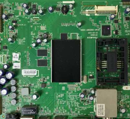
Solder joint quality is the most important part in PCBA processing. The reliability of solder joint quality determines the reliability and service life of PCBA products. Once the solder joint fails, the PCBA will be repaired or scrapped. Improving the reliability of solder joint is one of the processing goals of electronic processing plant. Next, Shenzhen PCBA processing manufacturer -kingford will introduce the causes and solutions of PCBA welding spot failure.
The main reason of solder joint failure in PCBA processing
1. Bad pin of components: the pin is polluted or oxidized, leading to solder joint failure.
2. PCB welding pad is bad: the coating is polluted, the surface is oxidized and warping occurs.
3, solder quality defects: unreasonable composition, excessive impurities, oxidation phenomenon.
4. Flux quality defects: low weldability, low efficiency, high corrosion.
5, process parameter control defects: unreasonable design, poor process control, equipment debugging deviation.
6, other auxiliary material defects: such as adhesive, cleaning agent quality problems, etc.
PCBA processing solder joint failure solution
1, reliability test work, that is, reliability test and analysis of PCBA processing solder joints, the main purpose is to analyze and identify the reliability of PCBA solder joints and provide reference parameters for processing;
2. Improve the reliability of solder joints in the processing process, carefully analyze the failure solder joints and find out the causes of failure, and then modify and improve the design process, structural parameters, welding process, improve the PCBA processing yield.

2. What does DIP plug-in mean? What should we pay attention to in DIP plug-in processing?
DIP plug-in processing is a process in the circuit board processing of plug-in devices. According to the different plug-in devices, it is divided into manual plug-in and machine plug-in. Next, I will introduce the meaning of DIP plug-in. What should we pay attention to in DIP plug-in processing?
What does DIP plugin mean?
DIP (Dual in-line Package), also known as dual-in-line package technology, refers to integrated circuit chips packaged In dual-in-line format. Most small and medium-sized integrated circuits are packaged in this format, and the number of pins is generally less than 100. The DIP-packaged CPU chip has two rows of pins that need to be plugged into the chip socket that has the DIP structure. Of course, it can also be inserted directly into the circuit board with the same number of welding holes and geometric arrangement for welding. Special care should be taken when inserting and removing the DIP encapsulated chips from the chip socket to avoid damaging the pins. DIP packaging structure forms are: multi-layer ceramic double-in-line DIP, single-layer ceramic double-in-line DIP, lead frame DIP (including glass ceramic sealing type, plastic encapsulation structure type, ceramic low-melt glass packaging type), etc.
DIP plug-in processing precautions
1. Wear protective devices such as electrostatic bracelets and finger covers.
2. Prepare the materials in advance, put the materials in the designated box, stick the label to prevent mixing, and preview and get familiar with their work content in advance.
3. Insert the parts to be placed into the corresponding feet on the PCB board, and pay attention to the front and back sides of the parts, close to the board surface.
4. Gently press the parts by hand to ensure that the parts are placed in place, and check whether the parts have floating height, skew, polar reverse and other errors and leakage phenomena.
5. Check the inserted components and remove errors and defective components in time.
6. Due to frequent manual errors and missed detection, Jingbang Electronics has introduced the world's advanced and accurate measurement technology, which can measure components from various angles to obtain 3D images, so as to carry out damage safety and high-speed defect detection. It can quickly detect the height, position, wrong parts, missing parts, foreign bodies, parts warping, BGA warping, detection and other adverse phenomena, greatly improving the working efficiency of the plug-in.
7. Clean the dirty motherboard after the wave soldering furnace.
8. The lead Angle of the parts is exposed too long to trim, pay attention not to scratch the circuit board.
9. The quality of the motherboard inspection and testing, has been to ensure the reduction of product defect rate. So a complete circuit board is produced.
There are four reasons to choose kingford for PCBA processing
1. Strength assurance
▪ SMT workshop: We have imported SMT machines and a variety of optical testing equipment, capable of producing 4 million pieces per day. Every process is equipped with QC personnel who can keep a close eye on product quality.
▪ DIP production line: There are two wave welding machines. Among them, there are more than ten old employees who have worked for more than three years. Skilled workers can weld all kinds of insert materials.
2. Quality assurance, high cost-effective
▪ High-end equipment can mount precision heterosexual parts, BGA, QFN, 0201 materials. Proofing can be machine paste, also can be hand pendulum.
▪ Samples and large and small batches can be produced. Proofing starting price 800 yuan, batch starting price 0.008 yuan/point, no start-up fee.
3. Rich experience in SMT and welding of electronic products, stable delivery time
▪ Has served thousands of home appliance subsidiaries, involving various kinds of automotive equipment and industrial control motherboard SMT SMT processing services. Products are often exported to Europe and the United States, the quality of new and old customers affirmed.
▪ On time delivery, usually within 3-5 days after the board is assembled, small batch expedited can also be shipped on the same day.
4. Strong maintenance ability and perfect after-sales service
▪ Experienced maintenance engineers are able to repair defective products caused by various welding problems and ensure the connectivity rate of each circuit board.
▪ 24-hour customer service staff will be ready to respond and resolve your order as soon as possible.


Just upload Gerber files, BOM files and design files, and the KINGFORD team will provide a complete quotation within 24h.