
Professional PCB manufacturing and assembly
Building 6, Zone 3, Yuekang Road,Bao'an District, Shenzhen, China
+86-13410863085Mon.-Sat.08:00-20:00

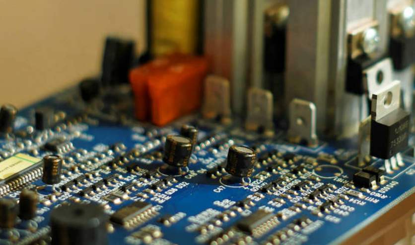
Because the printed circuit board has the unique advantages of high reliability, high density, strong design, strong production, more and more widely used in our life electronic equipment, a good quality electronic equipment, largely depends on its PCB quality, so how to know the quality of the circuit board?
1. Main tools: magnifying glass or calibration microscope. The most traditional inspection method is to use the operator's visual inspection to determine whether the board is unqualified and when it needs to be corrected. This method has the advantages of low cost, but it also has some disadvantages such as large subjective error, high long-term cost, discontinuous defect detection and difficult data collection. As PCB output increases, PCB line spacing and component size become smaller, and the disadvantages of this approach become more and more obvious.
2. Main tools: needle bed tester, flying needle tester. Detect manufacturing defects by testing electrical performance and testing analog, digital, and mixed-signal components to ensure they meet specifications. Its advantages are low testing cost per PCB board, strong digital and functional testing capabilities, short circuit and open circuit testing fast and thorough, programming firmware, high defect coverage, simple programming. Of course, its disadvantages are the need to test fixture, programming debugging time is long, the cost of making fixture is high, the use of more difficult problems.
3. Functional system testing is to use special testing equipment in the middle and end of the production line to carry out a comprehensive test on the functional modules of the circuit board to confirm the quality of the PCB circuit board. Functional testing can be said to be the earliest principle of automatic testing. It is based on specific circuit boards or specific units and can be completed by various devices. There are final product tests, up-to-date physical mock-ups, and stack tests. Functional testing typically does not provide in-depth data, such as foot - and component-level diagnostics for process improvement, and requires specialized equipment and specially designed test procedures. The complexity of writing functional test programs makes them unsuitable for most PCB production lines.
4, automatic optical detection Automatic optical detection is also known as automatic visual detection. This method is based on the optical principle and combines image analysis, computer and automatic control technology to detect and deal with the defects encountered in production. This is a relatively new method of manufacturing defect confirmation. AOI is generally used before and after backflow and before electrical testing to improve the pass rate during the electrical handling or functional testing phase. At this point, the cost of fixing the defect is much lower than the cost after the final test, often up to ten times higher.
5, laser detection system is the latest development of PCB detection technology. It uses a laser beam to scan the printed board, collect all the measurements, and compare the actual measurements to a preset qualifying limit. The technology has been proven on lightweight plates, is being considered for assembly plate testing, and is fast enough to be used on volume production lines. Its main advantages are fast output, no fixture required, visible maskless access; High initial cost, maintenance and use problems are the main disadvantages.
6. Main tools: binary image measurement. Measurement hole position, length, width, position and other dimensions. As the circuit board belongs to "small, thin and soft" products, the contact measurement is easy to produce deformation, resulting in inaccurate measurement, so the binary image measurement instrument becomes the best high-precision dimensional measurement instrument.
7. Automatic X-ray inspection can see through the parts to be tested and find defects by using different absorptivity of different substances to X-ray. It is mainly used to detect the defects of ultra-fine spacing and ultra-high density circuit boards and the defects of bridging, missing pieces and poor alignment in the assembly process. The tomographic imaging technology can also be used to detect the internal defects of IC chips. It is the only method to test the welding quality of ball grid array and shielded tin ball. The main advantage is the ability to detect BGA welding quality and insert components without fixture cost.
New design PCB board find fault method to share
Mar 04,2023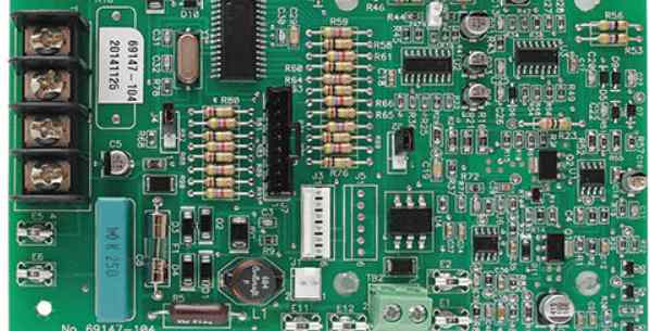


Just upload Gerber files, BOM files and design files, and the KINGFORD team will provide a complete quotation within 24h.