
Professional PCB manufacturing and assembly
Building 6, Zone 3, Yuekang Road,Bao'an District, Shenzhen, China
+86-13410863085Mon.-Sat.08:00-20:00

At present, the PCB circuit board products on the market are mainly divided into three kinds from the material categories: ordinary substrate, metal substrate and ceramic substrate. Next, Shenzhen PCB Board factory -kingford introduces common metal substrate classification and its advantages.
1, the classification of common metal substrate:
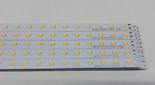
There are three main types of metal substrate: aluminum substrate, copper substrate, iron substrate. Here the key analysis is aluminum substrate, copper substrate.
Aluminum substrate is the most used substrate in metal substrate at present, with good thermal conductivity, electrical insulation and mechanical properties. Aluminum substrate is divided into flexible aluminum substrate, mixed aluminum substrate, multilayer aluminum substrate, through hole aluminum substrate, etc.
Copper substrate is one of the most expensive metal substrate, its thermal conductivity is many times better than aluminum substrate and iron substrate. Copper substrate is divided into gold plating copper substrate, silver plated copper substrate, tin spray copper substrate, copper oxide substrate, etc.
2, the advantages of metal substrate:
1. Thermal expansibility
The metal substrate can effectively solve the problem of heat dissipation, so that the problem of thermal expansion and contraction of different substances on the circuit board can be alleviated, and the durability and reliability of electronic equipment can be improved.
2, heat dissipation
At present, many double panel, multilayer board high density, power, heat distribution is difficult; Metal - based printed board can solve the problem of heat dissipation.
3. Dimensional stability
The metal substrate size is much more stable than that of the insulating material.

4. A wide range of applications
Aluminum substrate has a wide range of applications, such as audio equipment input, output amplifier, balance amplifier; Computer CPU board floppy disk drive, power supply device; Automotive electronic regulator, igniter, power controller; Lamps and lanterns, LED lights, etc.
Copper substrate is mainly suitable for high frequency circuit, including high temperature and low temperature in the area of precision communication equipment heat dissipation.
My company metal substrate technology ability
Layers: 1-2L (metal substrate & metal core board), 1-2L (ceramic DBC board);
Plate thickness: 0.5-3.0mm Size: max:400*500,min:25*25mm;
Machining: X/Y/Z accuracy ±0.08mm, horn hole, screw hole;
Thermal conductivity of thermal conductivity materials: conventional thermal conductivity materials: 1-4W/m.k; Ceramic thermal conductivity material: 24-170W/m.k;
Maximum wiring copper thickness: 5OZ;
Metal surface treatment: ordinary oxidation of aluminum, aluminum hard oxidation, aluminum chemical passivation, sandblasting, wire drawing, surface electroplating treatment;
Surface treatment process: hot air leveling, chemical precipitation, tin precipitation, silver precipitation, electroplating soft/hard gold, etc.
2.PCB design wiring measures to reduce high-frequency signal crosstalk
The parameters of PCB board layer, the distance between signal wires, the electrical characteristics of driver end and receiver end and the connection mode of signal wires have certain influence on the crosstalk.
PCB design to reduce high frequency signal crosstalk routing measures
1. Insert a ground or ground plane between two lines with serious crosstalk to isolate and reduce crosstalk;
2. If the parallel distribution cannot be avoided, a large area of "ground" can be arranged on the opposite side of the parallel signal line to greatly reduce interference;
3. On the premise of allowing wiring space, the spacing between adjacent signal lines can be increased to reduce the parallel length of signal lines;
4. If parallel cabling on the same floor is unavoidable, the direction of cabling on the two adjacent floors is vertical;
5. The clock line is surrounded by ground lines, and more ground holes are made to reduce capacitance distribution and crosstalk;
6. For high frequency signal clock, try to use low voltage differential minute signal and wrap;
7. Do not hang the idle input, but ground it or connect it to the power supply.
PCBA processing service flow
1. Project consultation/quotation: Customers provide complete PCBA information quotation;
2. Customers place orders: customers confirm the quotation, sign the contract and pay the advance payment;
3. Engineering evaluation: engineering evaluation customer to provide data, into the final means of production;
4. Procurement of raw materials: arrange PCB board and component procurement according to production materials;
5. PCBA production: SMT and DIP welding will be carried out after the plate and material are assembled;
6. PCBA test: test products according to customer requirements;
7. Packaging and after-sales service: The customer pays the balance, and PCBA packages and delivers the goods.


Just upload Gerber files, BOM files and design files, and the KINGFORD team will provide a complete quotation within 24h.