
Professional PCB manufacturing and assembly
Building 6, Zone 3, Yuekang Road,Bao'an District, Shenzhen, China
+86-13410863085Mon.-Sat.08:00-20:00

In the production process of PCBA patch processing, sometimes there will be white spots or white spots on the PCBA board. This phenomenon belongs to the processing defect and will affect the quality of PCBA board. Next, kingford, Shenzhen PCBA OEM manufacturer, will introduce why white spots are produced in PCBA processing and the solutions to produce white spots.
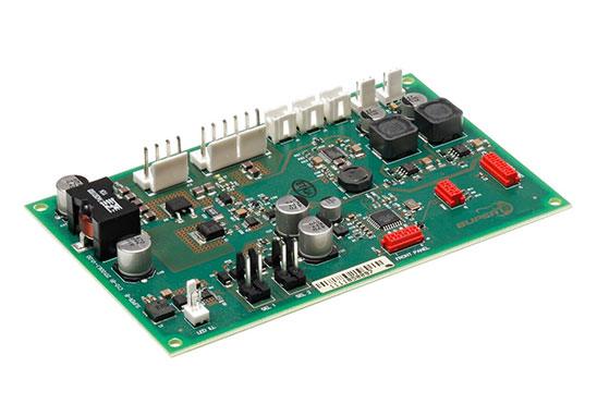
Shenzhen PCBA OEM processing factory
Causes of white spots in PCBA processing
1. The circuit board is subjected to inappropriate thermal stress;
2. Due to the influence of mechanical force, part of the resin is separated from the glass fiber, forming white spots;
3. Some PCBA processing equipment has been immersed in fluoride and etched fiberglass cloth, forming regular white spots.
PCBA processing to produce white spot solution
1. Strictly control the parameters of hot air distillation, infrared hot melt and other process links;
2. Reduce the external force of the machine. During PCBA SMT processing, measures should be taken to reduce excessive machine vibration.
2. Introduction of steel mesh scrubbing process for SMT patch processing
In the process of SMT patch processing and production, due to a series of reasons such as PCB substrate deformation, inaccurate positioning, support is not in place, design and so on, it is difficult to form an ideal seal between the steel mesh and the solder pad of PCB substrate in the process of solder paste printing. In the solder paste printing process of SMT processing, there will always be some solder paste extruded from the gap between the steel mesh and PCB to attach to the bottom of the steel mesh. If these solder paste is not processed in the follow-up PCBA processing, it will affect the surface cleaning of the circuit board and even the open side wall will adhere to the solder paste, affecting the transfer of the solder paste, so scrubbing the residual solder paste at the bottom of the steel mesh is an essential process in this processing link. The following to share a simple SMT patch processing steel mesh scrubbing process.

SMT patch processing steel mesh scrubbing technology
In SMT patch processing, we generally use automatic scrubbing method to clean. The modes of scrubbing include wet scrubbing, vacuum scrubbing and dry scrubbing. The combination process of wet scrubbing and vacuum scrubbing is usually adopted, that is, wet scrubbing first, then vacuum scrubbing and dry scrubbing. It can also use the combination of wet wipe and vacuum wipe. The purpose of wet rubbing is to remove residual solder paste from the bottom of the template, while the purpose of dry rubbing is to remove residual cleaning agent and flux from the bottom. The vacuum wipe nominally hopes to absorb the residual solder paste in the opening of the printing template, but the actual efficacy depends on the proportion of the opening area of the template. The possible effective function is to absorb the cleaning agent infiltrated into the hole wall, so as not to affect the first printing effect after wiping the net.
In the actual PCBA processing, besides the automatic cleaning function, it also needs to carry out regular manual cleaning. Because in the process of long-term printing of a large number of solder paste, the bottom of the steel mesh components will be contaminated, so as to form a hard scab around the mesh, and this thing is the need for processing personnel to manually remove regularly.
Generally, after artificial wet wipe, dry wipe or place for a few minutes, otherwise it may lead to the first one or two plates under the tin is not good. Because the manual wiping net is wet, too much cleaning agent penetrates into the opening hole wall, and the rapid volatilization of cleaning agent leads to the increase of solder paste viscosity, which affects the solder under the SMT patch.
kingford specializes in providing overall PCBA electronic manufacturing services, including upstream electronic component procurement to PCB production and processing, SMT patches, DIP plug-ins, PCBA testing, finished product assembly and other one-stop services.
The company gives full play to its competitive advantages in scale procurement and quality control, and has signed long-term cooperation agreements with many electronic component manufacturers at home and abroad and around the world to ensure the quality and stable supply of raw materials, and transfer the benefits to customers.
How can SMT machining avoid printing failure?
Mar 01,2023


Just upload Gerber files, BOM files and design files, and the KINGFORD team will provide a complete quotation within 24h.