
Professional PCB manufacturing and assembly
Building 6, Zone 3, Yuekang Road,Bao'an District, Shenzhen, China
+86-13410863085Mon.-Sat.08:00-20:00

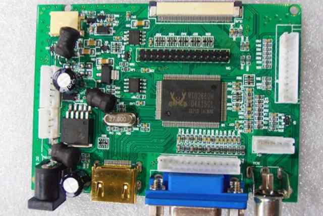
In order to meet customer requirements, the circuit board must be plugged through the Via hole. After a lot of practice, the traditional aluminum sheet plugging process is changed, and the circuit board surface welding and plugging are completed with white mesh. Stable production and reliable quality.
The Via hole plays the role of connecting the lines to each other. The development of the electronics industry also promotes the development of PCB, which also puts forward higher requirements for the production process and surface mounting technology of printed board. Via hole plugging technology comes into being and should meet the following requirements:
1. Copper can be found in the through hole, and welding resistance can be plugged or not plugged;
2. Through the hole must have tin lead, there is a certain thickness requirements (4 microns), no solder ink into the hole, resulting in the hole hidden tin beads;
3. The pass-through hole must have solder resistance ink plug hole, light proof, no tin ring, tin beads and flat requirements.
The function and process of PCB board making through hole plug are introduced
With the development of electronic products to "light, thin, short, small" direction, PCB also to high density, high difficulty development, so there are a large number of SMT, BGA PCB, and customers in SMT processing requirements plug hole, mainly has five functions:
1. Prevent short circuit caused by tin penetrating through the component surface from the passthrough hole during wave soldering of PCB; In particular, when we put the hole on the BGA pad, we must first do the plug hole, and then gold-plated treatment, to facilitate the welding of BGA.
2. Avoid flux residue in the pass hole.
3. After the surface mounting and component assembly in the electronics factory is completed, the PCB should be vacuums to form negative pressure on the testing machine.
4. Prevent the surface solder paste from flowing into the hole to cause virtual welding, affecting the installation.
5. Prevent over wave soldering tin bead pop out, resulting in short circuit.
The realization of conductive hole plugging process
For the surface mounting plate, especially the mounting of BGA and IC, the requirements for the through-hole plug hole must be flat, convex and concave plus or minus 1mil, and the edge of the through-hole shall not be red and tinned; Through the hole hidden tin beads, in order to meet customer requirements, through the hole plugging process is all over the place, the process is particularly long, process control is difficult, often in hot air leveling and green oil soldering resistance experiment oil loss; Problems such as oil explosion occur after curing.
Now according to the actual conditions of production, the PCB plugging process is summarized, in the process and advantages and disadvantages of some comparison and description: Note: the working principle of hot air smoothing is to use hot air to remove the excess solder on the surface of the printed circuit board and the hole, the remaining solder uniformly covered in the solder plate and open solder line and surface seal decoration, is one of the ways of surface treatment of the printed circuit board.

2. What is PCB quick proofing?
PCB Rapid proofing is a circuit board proofing service that is designed, manufactured, assembled and tested in a short period of time in an accelerated process. Production times can vary from 24 hours to 7 days, depending on the complexity of the design.
PCB rapid proofing goes through three production stages.
Prototype stage
Building a prototype PCB contains all the vague requirements and details needed to reduce delivery time and manufacturing costs. In addition, PCB prototypes allow users to test how the finished product works. It enables customers to make required changes while manufacturers can check for faults to improve performance and efficiency.
Therefore, corrections, omissions, corrections, additions and subtractions are captured in this phase to ensure that the PCB is manufactured with zero technical or mechanical defects.
Test run/pre-production
The beta run involves building fast flip boards in batches of hundreds to thousands of pieces. This is one of the most important stages in the process, as these PCB templates are usually turned into the final product. So manufacturers have to eliminate all errors at this stage.
This process requires electrical testing, optimizing circuit board layout, checking tool arrangements, avoiding traps, etc.
Full-scale production
The final stage of production is rapid PCB manufacturing for market applications. This stage of the order is higher and better than the other steps, but may take longer to complete.
Only after the design and engineering teams have completed the previous phase to fine tune everything and build high quality boards can a rapid shift to PCB manufacturing be achieved.
The factors affecting PCB fast proofing time
The time to market for PCB rapid proofing depends on a number of factors, such as the following.
Design and test procedures
Adherence to DFM and DFT guidelines reduces completion time and provides high quality boards. Also, check the availability of components before including them in your design and determine the best layout strategy for your compact design. Finally, establish clear testing protocols and requirements ahead of time to reduce turnaround time.
Lamination period
High density interconnected (HDI) boards with multiple perforated structures require sequential laminating cycles, a task similar to manufacturing multilayer panels. This type of board adds time, cost, and complexity to manufacturing.
The time required for each lamination cycle depends on the number of board layers in the stack and the materials used. Each individual layer adds an average of 4-5 days to the production process, including drilling, filling and plating time. And circuit board makers need at least an extra day to process the outer layer.
Via-in-Pad plating
Through-holes in pads have become typical applications in most PCBS because they keep heat away from the lower part of the element or save space. However, merging them adds at least one day to the cycle time.
Manufacturing drawing specification
Manufacturing diagrams represent important manufacturing data, as shown below.
- Industrial control level
- Mechanical dimensions
- Through the drill chart
- Layer on top of each other
- Plating thickness
Therefore, you need to understand the PCB manufacturer's ability to close the gap between the design document and the DFM in order to reduce or avoid rework time delays. Always mention whether the prototype complies with IPC Class 2 or Class 3 manufacturing standards.
Similarly, multilayer PCB lamination is performed while considering material cost and availability. Rare materials will take more time to procure, increasing turnaround time. During this time, the controlled impedance table of the plot is verified to ensure that it identifies the line width and target impedance that need to be controlled to avoid delays due to information mismatches.
Surface treatment
Finishing is also time consuming, as each coat takes a specific amount of time to complete. For example, ENIG takes about 1.5-2 hours to complete, while HASL takes only 15-20 minutes at most.
As a result, it will take more time to complete high quality PCBS with two finishes, such as ENIG for surface mount connectors and hard gold for edge connectors. Each finish is applied individually and the time will add up.
Assembly drawing and manufacturing instructions
Manufacturing instructions and assembly drawings help with board inspection because they contain part lists, bottom and top views, shapes, and so on. So consider the following points to prevent delays during board assembly.
- Follow the DFA guidelines and verify that component footprints do not match
- If parts are supplied, follow the accompanying guide
- Ensure that the silk screen feature marks remain visible
- Send the complete BOM containing the manufacturer part number and product description
Factors to consider when selecting PCB rapid proofing manufacturing partner
Circuit board manufacturing is a complex process. Getting it done faster requires more attention, so be sure to consider these factors before choosing a PCB quick proofing manufacturer.
experience
Rapid prototyping and production requires experience if the final product is to be functional and of high quality. Therefore, consider a manufacturer/assembler with a good reputation in the market.
speed
Also, consider the lead time before handing over the design. Some manufacturers can complete the process in 24 hours, while others can do it in a few days. But faster isn't always better. The key factor is to ensure that the manufacturer's speed fits your schedule. Short-term production is usually more expensive.
equipment
Any PCB fast proofing manufacturer should have the equipment to make high quality boards faster. You can ask them for a list of equipment, but the sure way is to go to the factory and see for yourself.
quality
Manufacturers should pay more attention to quality rather than speed, so high-speed manufacturing should not affect product quality. Ideally, this partner should have quality control process certification.
Shenzhen Honglijie not only has a number of certification, and we also have a number of well-known customers. This combination assures you of our quality in PCB manufacturing and assembly.
cost
The cost is high because you can only close the deal if the offer is within your budget. Cheap is not always best because quality can be compromised. So try to get a good deal through quality assurance.
How to determine the PCB substrate material?
Feb 23,2023


Just upload Gerber files, BOM files and design files, and the KINGFORD team will provide a complete quotation within 24h.