
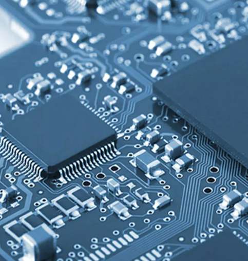
Professional PCB manufacturing and assembly
Building 6, Zone 3, Yuekang Road,Bao'an District, Shenzhen, China
+86-13410863085Mon.-Sat.08:00-20:00

There are two ways to make the high-speed circuit work on the relatively long line without serious waveform distortion. TTL adopts Schottky clamping method for the fast falling edge, so that the overimpulse is clamped at a level one diode voltage drop lower than the ground potential, which reduces the backkick amplitude behind, and the slow rising edge allows overimpulse. But it is attenuated by the relatively high output impedance (50 to 80Ω) of the circuit in the level "H" state. In addition, due to the high immunity of the level "H" state, the recoil problem is not very prominent. For HCT series devices, if Schottky diode clamping and series end method are combined, the improvement effect will be more obvious.
When there is a fan out along the signal line, the TTL shaping method described above appears to be somewhat insufficient under the condition of higher bit rate and faster edge rate. Because there are reflected waves in the line, they tend to be synthesized at high speed, which leads to serious signal distortion and reduced anti-interference ability. Therefore, in order to solve the reflection problem, another method is usually used in ECL systems: line impedance matching method. In this way, the reflection can be controlled and the integrity of the signal can be guaranteed.
Strictly, he says, transmission lines are not needed for conventional TTL and CMOS devices with slower edge speeds. Transmission lines are also not always needed for high-speed ECL devices with faster edge speeds. But when transmission lines are used, they have the advantage of predicting line delay and controlling reflection and oscillation through impedance matching.
1. The basic factors that determine whether to use a transmission line:
(1) the speed along the system signal;
(2) connecting distance;
(3) capacitive load (how much fan out);
(4) resistive load (terminal mode of line);
(5) Allowable recoil and overshoot percentage (reduction degree of AC immunity).
2. Several types of transmission lines
(1) Coaxial and twisted pair wires: They are often used for system to system connections. The characteristic impedance of coaxial cable is usually 50Ω and 75Ω, and twisted pair is usually 110Ω.
(2) Microstrip line on the printed circuit board: microstrip line is a strip guide (signal line). It is separated from the ground plane by a dielectric. If the line's thickness, width, and distance from the ground plane are controllable, so is its characteristic impedance. The characteristic impedance Z0 of microstrip line is:
(3) Strip line in PCB circuit board: Strip line is a copper strip line placed in the middle of the dielectric between two layers of conductive plane. If the thickness and width of the line, the dielectric constant of the medium and the distance between the two conducting planes are controllable, then the characteristic impedance of the line is also controllable. The characteristic impedance of the strip line is:
3. End the transmission line
When the receiving end of a line is connected with a resistance equal to the characteristic impedance of the line, the transmission line is said to be connected in parallel. It is mainly used for obtaining the best electrical performance, including driving distributed loads.
Sometimes in order to save power consumption, a 104 is connected to the resistance of the opposite end to form an AC terminal circuit, which can effectively reduce DC loss.
A resistance is connected in series between the driver and the transmission line, and the end of the line is not connected to the resistance. This method of terminating is called series terminating. Overshoot and ringing on longer lines can be controlled by series damping or series terminating techniques. Series damping is achieved using a small resistance (typically 10 to 75Ω) in series with the output of the driver door. This damping method is suitable for use in connection with lines whose characteristic impedance is controlled (such as baseboard wiring, ground-less circuit boards and most wound wiring, etc.).
The sum of the value of the series resistance and the output impedance of the circuit (driving gate) at series terminations is equal to the characteristic impedance of the transmission line. Series terminal connection has the disadvantages of lumped load only at the terminal and long transmission delay time. However, this can be overcome by using redundant series terminating transmission lines.
4. Unterminated transmission line
If the line delay time is much shorter than the signal rise time, the transmission line can be used without series terminating or parallel terminating. If the double delay of a non-terminal line (the time it takes the signal to make one round trip on the transmission line) is shorter than the rise time of the pulse signal, then the recoil due to non-terminating is about 15% of the logical swing.
5. Comparison of several terminating modes
Both parallel terminal connection and series terminal connection have their own advantages. Whether to use one or both depends on the designer's preference and the requirements of the system. The main advantages of the parallel terminal connection are the high speed of the system and the complete signal transmission on line without distortion. The load on the long line will neither affect the transmission delay time of the driving gate driving the long line nor affect its signal edge speed, but will increase the transmission delay time of the signal along the long line. When driving a large fan out, the load can be distributed along the branch short line, rather than the terminals where the load must be lumped online as in series terminations.
The series terminal method enables the circuit to drive several parallel load lines. The delay time increment caused by the series terminal connection due to the capacitive load is about twice as large as that of the corresponding parallel terminal connection, while the edge speed is slowed down and the driving gate delay time is increased for the short line due to the capacitive load. However, the crosstalk of the series terminal connection is smaller than that of the parallel terminal connection. The main reason is that the signal amplitude transmitted along the series terminal is only half of the logical swing, and therefore only half of the switch current connected in parallel, small signal energy crosstalk is small.
Do PCB board is to choose double panel or multilayer board, depends on the highest working frequency and the complexity of the circuit system and the requirements of assembly density to decide. When the clock frequency exceeds 200MHZ, it is best to choose multilayer board. If the working frequency is more than 350MHz, it is best to use PTFE as a dielectric layer printed circuit board, because its high frequency decay is smaller, parasitic capacitance is smaller, transmission speed is faster, but also due to Z0 larger and power saving, the printed circuit board routing has the following principles:
(1) A large interval should be left between all parallel signal lines as far as possible to reduce crosstalk. If there are two signal cables that are close to each other, it is best to route a ground cable between the two cables to shield them.
(2) The design of signal transmission line to avoid sharp bends, in order to prevent the transmission line characteristic impedance mutation and reflection, to try to design into a certain size of the uniform arc line.
(3) The width of the printed line can be calculated according to the characteristics of the microstrip line and strip line. The characteristic impedance of the microstrip line on the printed circuit board is generally between 50 and 120Ω. To obtain large characteristic impedance, the linewidth must be made very narrow. But very thin lines are not easy to make.
Considering various factors, it is generally appropriate to choose an impedance value of about 68Ω, because the choice of 68Ω characteristic impedance can achieve the best balance between delay time and power consumption. A 50Ω transmission line will consume more power; Larger impedance can reduce the power consumption, but it will make the transmission delay time abhorrent. Due to the negative capacitance, the transmission delay time will be increased and the characteristic impedance will be decreased. However, the intrinsic capacitance per unit length of line segment with very low characteristic impedance is larger, so the transmission delay time and characteristic impedance are less affected by the load capacitance.
An important characteristic of a properly terminated transmission line is that branching short lines should have little effect on line delay time. When Z0 is 50Ω. The length of branching short lines must be limited to 2.5 cm. To avoid loud ringing.
(4) For double-sided circuit board (or six layers of the board to take four lines). The lines on both sides of the board should be perpendicular to each other to prevent cross-talk induced by each other.
(5) If the printed board is equipped with large current devices, such as, horn, etc., their ground wires should be separated separately to reduce the noise on the ground wire. The ground wires of these large current devices should be connected to an independent ground bus on the plug-in board and the backplane, and these independent ground wires should also be connected with the ground point of the entire system.
(6) If there is a small signal amplifier on the board, the weak signal line should be far away from the strong signal line before amplification, and the line should be as short as possible, and if possible, it should be shielded by the ground line.


Just upload Gerber files, BOM files and design files, and the KINGFORD team will provide a complete quotation within 24h.