Background technology:
With the rapid development of electronic industry, the global PCB industry has been the rapid development, as a big country of PCB production, about 40% of the world's output, but also the rapid development. In particular, the appearance of High Density Interconnect Technology (HDI) promotes the continuous innovation of various electronic devices, especially the rapid upgrading of intelligent electronic devices in recent years. The printed circuit board products in the multi-function, high integration, thinner, lighter, smaller and other aspects put forward more and higher technical innovation requirements, promote the PCB products to thinner and thinner thickness, more and more layers, wiring more and more thin, more and more dense, can be any layer interconnection direction development. "Light, thin, short, small, high density, high difficulty" is the main development trend of PCB products at present.
In the manufacturing process of HDI circuit board, there are many defects and difficulties in the process, among which the most important problems are that the blind hole sag can not be routed, the blind hole can not be transferred to form the circuit and so on.

Technology implementation elements:
To solve the above problems, the invention provides a blind hole wiring method for HDI circuit board, which saves more than 20% of wiring space, improves wiring density, and realizes miniaturization and lightweight of electronic products.
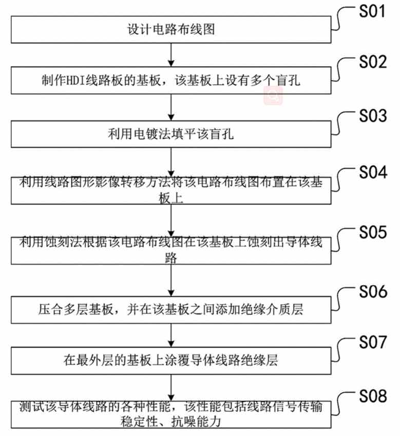
The technical scheme to achieve the above purpose is: a blind hole wiring method for HDI circuit board, including the following steps,
S01: Design circuit wiring diagram;
S02: a substrate for manufacturing HDI circuit board, which is provided with a plurality of blind holes;
S03: Use electroplating method to fill the blind hole;
S04: The circuit routing diagram is arranged on the substrate by using the line graphic image transfer method;
S05: A conductor line is etched on the substrate according to the circuit routing diagram by etching method.
Further, the blind hole wiring method for the HDI circuit board includes the following steps,
S06: Pressing a multilayer substrate and adding an insulating dielectric layer between the substrate;
Wherein, step S06 follows step S05.
Further, the thickness and distribution of insulating dielectric layers in step S06 are uniform.
Further, the blind hole wiring method for the HDI circuit board includes the following steps,
S07: The outermost substrate is coated with a conductor line insulation layer; Wherein, the step S07 follows the step S06.

Further, the thickness and distribution of the insulation layer in step S07 is uniform.
Further, the blind hole wiring method for the HDI circuit board includes the following steps,
S08: Test various performance of the conductor line, including the stability of signal transmission and anti-noise ability of the line; Among them, step S08 is completed in the last step.
Furthermore, the thickness and distribution of the electrodeposited coatings produced by electroplating method in the step S03 are uniform.
After adopting the invention, wiring space can be saved by more than 20%, wiring density can be improved, and electronic products can be miniaturized and lightweight. The blind hole electroplating and filling is smooth without dents, and the completed hyperfine conductor line is uniform without notches and convex spots, and the corresponding layer lines are well connected. The signal transmission is stable and the anti-noise performance is good.
Concrete implementation mode
Embodiment 1, a blind hole wiring method for an HDI circuit board. The HDI circuit board in this embodiment is a single layer board. The specific wiring method includes the following steps.
S01: Design the circuit wiring diagram. In the specific implementation, the circuit routing diagram passing through the blind hole should be designed first, and the production scheme should be designed according to the requirements of the laid circuit routing diagram. At the same time, the materials used should be selected and evaluated, and the thickness, width and thickness of the conductor and insulation layer should be pre-compensated during etching. Since the circuit wiring diagram is set according to the requirements of the product, there are no restrictions in this embodiment.
S02: A substrate for manufacturing the HDI circuit board. The substrate is provided with a plurality of blind holes. The location of the blind hole is set according to the requirements of the circuit. Blind hole design requirements meet the national standards, but also meet the design requirements. It includes transverse distance and longitudinal distance between blind holes.
S03: Fill the blind hole by electroplating. In the specific implementation, the thickness and distribution of the electroplating coating produced by electroplating method in the said step S03 are uniform, that is, the thickness and uniformity of the electroplating coating after the blind hole filling should be maintained. Electroplating adopts high depth capacity VCP circuit production line which is independently reformed and upgraded. During electroplating, the electroplating solution exchange in the blind hole is faster, the copper ion concentration distribution in the electroplating solution is more uniform, and the electroplating efficiency is higher. At the same time, the special electroplating solution combined with the modified special electroplating production line can make the blind hole electroplating fill more flat. Among them, the mechanism of blind hole filling electroplating solution: electroplating solution contains leveling agent, inhibitor, brightener, leveling agent control the copper atom crystal smooth, no disordered crystallization; Inhibitor: can greatly slow down the plating rate of the surface of the circuit board plating, and the plating rate in the hole is normal, so as to achieve the purpose of hole filling.
S04: The circuit routing diagram is laid out on the substrate using the line graphic image transfer method.
Specifically, the circuit routing diagram is transferred to the circuit board (substrate). Two methods are provided in this embodiment, as follows.
Method 1:
(1) The wiring diagram of the circuit board is transferred to the photographic film through the optical drawing machine.
(2) Press a layer of photosensitive resin film on the circuit board (substrate).
(3) Fix the negative with the circuit wiring diagram to the substrate with the photosensitive film pressed, and fix it through the preset positioning point.
(4) The substrate is placed in the exposure concentration for exposure with ultraviolet light, the light-permeable position of the photographic resin film on the negative is sensitized to curing, and the light-permeable position of the negative corresponding to the unexposed photographic film remains unchanged.
(5) Remove the negative, put the substrate into the developer, the unexposed part is developed away, exposing the copper layer under the sensitive film. The exposed resin film continues to adhere to the copper surface due to curing.
(6) Put the substrate into the etching potion, the copper layer without resin film protection is etched away, and the part protected by resin film is retained to form the required line due to the lack of contact with the potion.
Method 2:
(1) Press a layer of photosensitive resin film on the circuit board (substrate).
(2) Put the substrate into the LDI exposure concentration. The laser head in the exposure machine exposes the circuit wiring diagram on the sensitive film of the substrate like an inkjet printer, and the sensitive resin film at the exposure position is sensitive to curing.
(3) Put the substrate into the developer, and the unexposed part is developed away, exposing the copper layer under the sensitive film. The exposed resin film continues to adhere to the copper surface due to curing.
(4) Put the substrate into the etching potion, the copper layer without resin film protection is etched away, and the part protected by resin film is retained to form the required line due to the lack of contact with the potion.
S05: Etching method is used to etch a conductor line on the substrate according to the circuit routing diagram, and coating the conductor line insulation layer on the substrate.
After all the steps have been completed, the final inspection process is required.
S08: Test various performance of the conductor line, including the stability of signal transmission and anti-noise ability of the line; Among them, step S08 is completed in the last step.
Embodiment 2. The difference between this embodiment and Embodiment 1 is that the HDI circuit board in this embodiment is a multilayer circuit board. Therefore, the blind hole wiring method of the HDI circuit board in this embodiment also includes the following steps.
The following steps are also included after step S05 of Embodiment 1.
S06: Press a multilayer substrate and add an insulating dielectric layer between the substrate. In specific implementation, the thickness and uniformity of the insulating dielectric layer is controlled, that is, the thickness and distribution of the insulating dielectric layer in the step S06 is uniform.
S07: Coat the outermost substrate with a conductor line insulation layer.
Wherein, the step S07 follows the step S06. The insulation layer in step S07 has uniform thickness and distribution.


