
Professional PCB manufacturing and assembly
Building 6, Zone 3, Yuekang Road,Bao'an District, Shenzhen, China
+86-13410863085Mon.-Sat.08:00-20:00

Many DIY players will find the variety of PCB colors on the market bewildering. More common PCB colors are black, green, blue, yellow. Some PCB manufacturers have also developed different colors of white, pink, purple, red and brown PCB.
In the traditional impression, black PCB seems to be positioned at the high end, while red, yellow, etc., are dedicated to the low end. Is that true?
PCB copper layer without solder coating is easily oxidized when exposed to air
We know that both sides of PCB are copper layers. In the production process of PCB, whether the copper layer is made by addition method or subaddition method, it will eventually get a smooth and unprotected surface. Although the chemical properties of copper are not as active as aluminum, iron, magnesium, etc., but in the case of water, pure copper and oxygen contact easy oxidation; Due to the presence of oxygen and water vapor in the air, the surface of pure copper is quickly oxidized when exposed to air. The thickness of the copper layer in PCB is very thin, so the oxidized copper will become a bad conductor of electricity, which will greatly damage the electrical performance of the entire PCB.
To prevent copper oxidation, the welded and unwelded parts of the PCB are separated during welding. To protect the PCB surface, engineers have invented a special coating. The paint can be easily applied to the PCB surface to form a protective layer of a certain thickness that blocks the contact between the copper and the air. This coating is called a solder resistance layer, and the material used is solder resistance paint.
If it's called lacquer, it must have different colors. Yes, the original solder resistance paint can be made colorless and transparent, but for the convenience of maintenance and manufacturing of PCB circuit boards, it is often necessary to print small words on the board. Transparent solder resistance paint only exposes the background color of the PCB, so it is not good enough to be manufactured, repaired or sold. So engineers added a variety of colors to the solder stop layer, resulting in a black or red or blue PCB.
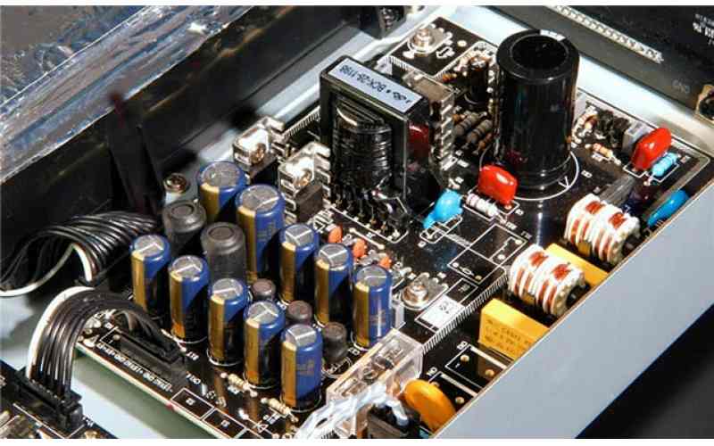
Black PCBS are difficult to see the wiring, which makes maintenance difficult
From this perspective, the color of the PCB has nothing to do with the quality of the PCB. Black PCBS are distinguished from other color PCBS such as blue and yellow PCBS by the color of the solder stop layer applied at the end. If the PCB design and manufacturing process is exactly the same, the color will not have any effect on the performance, nor will it have any effect on the heat dissipation.
For black PCB, its surface wiring is almost completely covered, which brings great difficulties to the later maintenance, so it is a color that is not easy to manufacture and use. Therefore, in recent years, people gradually reform, give up the use of black welding resistance paint, and instead use dark green, dark brown, dark blue welding resistance paint, so as to facilitate manufacturing and maintenance.
Having said so much, you have a basic understanding of the PCB color problem. The saying that "color represents high-end or low-end" is because manufacturers like to use black PCB for high-end products and red, blue, green and yellow for low-end products. The bottom line is that products give meaning to colors, not colors give meaning to products.
What are the benefits of using precious metals such as gold and silver on PCBS?
Now that the color is clear, let's talk about the precious metal on PCB. Some manufacturers in the promotion of their products, will specifically mention their products with gold plating, silver plating and other special processes. So what's the use of this process?
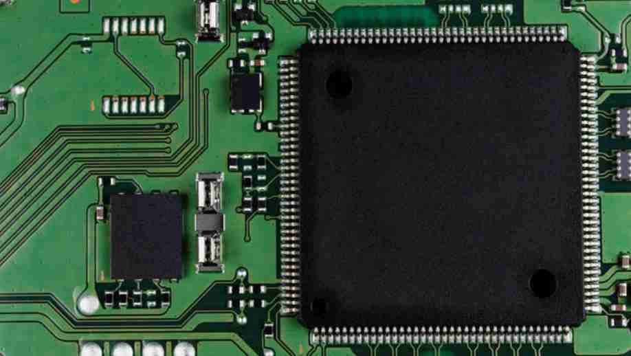
PCB surface needs to be welded components, so a part of the copper layer needs to be exposed for welding. These exposed layers of copper are called pads. The pad is generally rectangular or circular, and the area is small. To sum up, we know that the copper used in PCBS is easily oxidized, so the only thing exposed to the air after applying the solder stop layer is the copper on the pad.
If the copper on the pad is oxidized, it is not only difficult to weld, but also the resistivity will be greatly increased, seriously affecting the performance of the final product. So engineers came up with ways to protect the pad. For example, inert metal gold plating, or a layer of silver plating on the surface through a chemical process, or a special chemical film covering the copper layer, to prevent the pad from contact with the air.
Exposed pad on PCB, directly exposed copper layer. This part needs to be protected from oxidation
From this point of view, whether gold or silver, the purpose of the process itself is to prevent oxidation, protect the pad and ensure the yield in the subsequent welding process.
However, the use of different metals will require the storage time and storage conditions of PCB used in the production factory. As a result, PCB factories generally use vacuum plasticizers to pack PCBS after production and before delivery to customers to ensure maximum protection against oxidation.
Before the final component is machined, the board manufacturer must check the oxidation degree of the PCB once to remove the oxidized PCB and ensure the yield. In the end, the consumer gets a board that's been tested. Even after long-term use, oxidation almost only occurs in the insertion and removal of the connection parts, and has no effect on the welding pad and already welded components.
Since the resistance of silver and gold is lower, will the heat of PCB board be reduced after the use of silver and gold and other special metals?
We know that the biggest factor affecting the amount of heat produced is resistance. Resistance is related to the material of the conductor itself, the cross-sectional area of the conductor and its length. The thickness of the metal on the surface of the pad is even much less than 0.01 mm. If the pad is processed by OST (organic protective film), there will be no excess thickness. The resistance of such a small thickness is almost zero, which is incalculable, and of course does not affect the heat output.


Just upload Gerber files, BOM files and design files, and the KINGFORD team will provide a complete quotation within 24h.