
Professional PCB manufacturing and assembly
Building 6, Zone 3, Yuekang Road,Bao'an District, Shenzhen, China
+86-13410863085Mon.-Sat.08:00-20:00

PCB belongs to the basic industry of electronic information, which is greatly affected by the cyclical fluctuation of macro economy. At present, the global PCB enterprises are mainly distributed in China, Japan, South Korea and other places. The downstream application field of PCB industry is very wide, which is less affected by a single industry, so it is relatively dispersed, with many manufacturers, low market concentration and full market competition. In recent years, our country has become the largest PCB production area in the world, and there is a significant trend of iterative upgrading from low-end to high-end direction.
The construction of 5G commercial networks continued steadily. In the medium and long term, the general trend of 5G communication construction will not change. The Chinese government also proposed to "strengthen the construction of 5G network and gigabit optical network to enrich the application scenarios" when deploying the key work in 2021. Take routers, switches and other devices in the backbone network as an example. At present, the speed supported by a single interface (Port) of the mainstream specification is 100Gbps. As the data volume driven by 5G will grow multiple times, it will be popularized to 400Gbps, thus bringing the industry growth in the field of communication market board. Promote high frequency and high speed PCB products strong demand.
Car electronics bottoming out. Due to the impact of the epidemic, vehicle manufacturers have shut down their plants due to the unstable supply chain and sluggish market demand, and the market demand for automobile plates has declined significantly year-on-year. However, with the recovery of auto production, auto sales also rose from the bottom. In addition, the general trend of automobile electrification, intellectualization and networking is significant. Automotive electronics have strong demand for high-end PCB in the fields of advanced driver assistance systems (ADAS) and new energy vehicles, and the auto board market shows a V-shaped reversal trend and rapidly recovers.
In order to actively respond to market demand, the performance, technology and product structure of Chinese PCB products have been greatly optimized. From the perspective of product performance, Chinese PCB is developing towards the direction of high precision, high density and high reliability, with continuous improvement of performance and gradual popularization of professional, large-scale and green production mode. Dongshan Precision, Shennan Circuit and other Chinese PCB giants continue to optimize product structure to meet the needs of communication, server, storage, automotive electronics, consumer electronics and other application fields. From the perspective of technology and process, Chinese PCB enterprises have further increased their investment in technology research and development, focusing on high density interconnect board (HDI) and high speed and high frequency multilayer board technology. From the perspective of product structure, 8-16 layer multilayer board and 18 layer or more super high rise board have gradually replaced low level products in the Chinese PCB market, becoming the mainstream of the market.
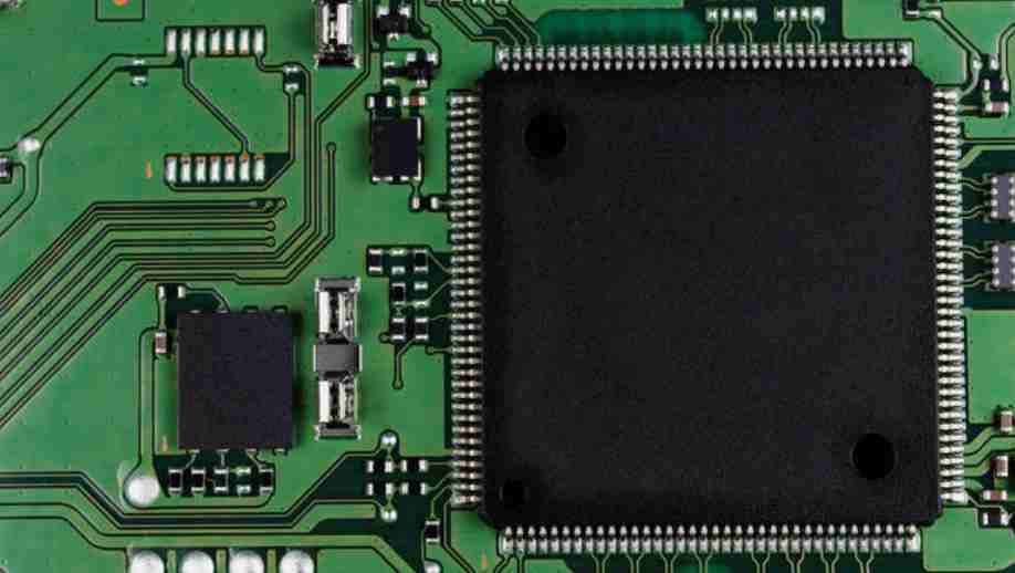
PCB circuit board is widely used in China. It will produce pollutants in the manufacturing process of printed circuit board, including dust and debris in the manufacturing process, such as residue of flux and adhesive. If the pcb board is not effectively guaranteed to clean the surface, resistance and leakage will cause the pcb board failure, thus affecting the service life of the product. Therefore, cleaning the pcb board during the manufacturing process is an important step.
Semi-water cleaning mainly uses organic solvent and deionized water, plus a certain amount of active agent, additive composition of cleaning agent. This cleaning is between solvent cleaning and water cleaning. These cleaners are organic solvent, flammable solvent, high flash point, low toxicity, safe to use, but must be rinsed with water and then dried.

Water purification technology is the development direction of clean technology in the future. It is necessary to establish pure water source and discharge water treatment workshop. Using water as cleaning medium, a series of water-based cleaning agents are formed by adding surfactants, auxiliaries, corrosion inhibitors and chelators in water. Water solvents and non-polar pollutants can be removed.
Used in the welding process without clean flux or clean solder paste, directly into the next process after welding cleaning, no longer free cleaning technology is currently the most commonly used alternative technology, especially mobile communication products are basically disposable methods to replace ODS. Solvent cleaning is mainly used for solvent dissolution to remove pollutants. Solvent cleaning requires simple equipment because of its fast volatilization and strong solubility.
The above four cleaning technologies can achieve a certain cleaning effect, but how to quickly and effectively clean pcb board? The application of ultrasonic cleaning machine can be solved. It uses ultra-high frequency to convert kinetic energy in the liquid medium to produce cavitation effect, forming countless tiny bubbles, and then impact the surface of the object, so that the surface dirt off, so as to achieve the effect of cleaning. Because it is through the liquid, as long as the liquid can touch the surface of the surface can be cleaned in place, leaving no dead space.
It can work on every surface of multiple objects simultaneously. It is very effective and fast and can be cleaned for about 15 minutes. One advantage of using ultrasonic cleaning is that it can effectively reduce the capacity of pads and components, and reduce electromagnetic interference.


Just upload Gerber files, BOM files and design files, and the KINGFORD team will provide a complete quotation within 24h.