
Professional PCB manufacturing and assembly
Building 6, Zone 3, Yuekang Road,Bao'an District, Shenzhen, China
+86-13410863085Mon.-Sat.08:00-20:00


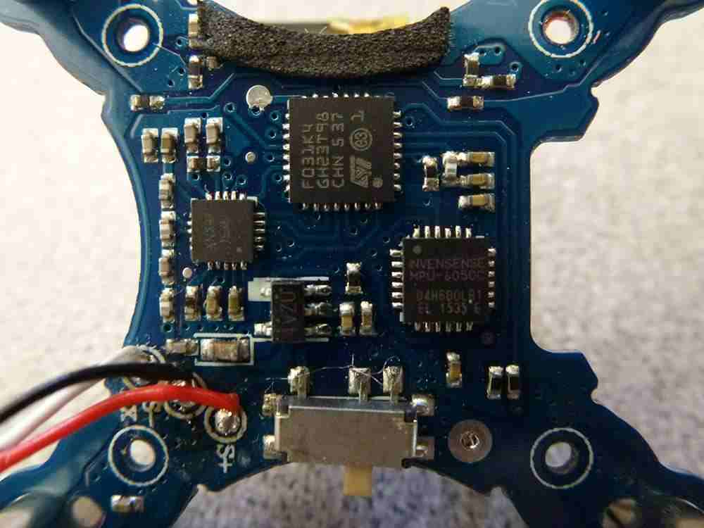
In PCB design, pad is a very important concept, PCB engineers must be familiar with it.
However, although familiar, many engineers on the pad knowledge is only a little. The types and design standards of pad in PCB design will be introduced in detail below.
Type of pad
Generally speaking, pad can be divided into seven categories, according to the shape of the distinction is as follows:
Square pad: printed board components are large but few, and printed wire is simple when used; The pad is easy to realize when making PCB by hand.
Round pad: widely used in single and double-sided printed boards with regular arrangement of components; If the density of the plate allows, the pad can be larger, welding will not fall off.
Island pad: the connection between the pad and the pad is integrated; It is often used in vertical irregular arrangement installation, such as radio tape recorder often used in the pad.
Teardrop type welding pad: when the welding pad is connected with a thin wire is often used to prevent the welding pad from peeling, wiring and welding pad disconnection; This pad is commonly used in high frequency circuits.
Polygon pad: Used to distinguish the outside diameter and different aperture pad, easy to process and assembly.
Oval pad: This pad has sufficient area to enhance stripping resistance. It is often used for dual-in-line devices.
Open shape pad: In order to ensure that after wave soldering, so that manual repair welding pad hole is not blocked by solder often used.
Design standard for shape and size of pads
(1) The minimum single side of all pads shall be no less than 0.25mm, and the maximum diameter of the whole pad shall be no more than 3 times of the component aperture.
② We should try to ensure that the spacing between the edges of the two pads is greater than 0.4mm.
(3) In the case of dense wiring, it is recommended to use oval and oblong connecting disks. The diameter or minimum width of single panel pad is 1.6mm; Double panel of weak current line welding pad only need to add 0.5mm hole diameter, welding pad is too large easy to cause unnecessary welding, aperture more than 1.2mm or pad diameter more than 3.0mm welding pad should be designed as diamond or plum shaped pad.
(4) For plug-in components, in order to avoid the phenomenon of copper foil breaking during welding, and single-sided connecting disk should be completely covered with copper foil; And double panel minimum requirement should fill tear drop.
⑤ The organic insert parts should be designed as dripping pads along the elbow to ensure that the solder joints at the elbow are full.
⑥ Large area of copper sheet on the pad should be chrysanthemum shaped pad, not to virtual welding. If the PCB has a large area of ground and power lines (more than 500 square mm), it should be partially windowed or designed to be filled with mesh.
PCB manufacturing process for welding pad requirements
(1) If the two ends of the patch component are not connected to the plug-in component, a test point should be added. The diameter of the test point is equal to or greater than 1.8mm, so as to facilitate online tester testing.
② If the IC foot pad with dense foot spacing is not connected to the hand plug-in pad, it is necessary to add a test pad. If it is a patch IC, the test point can not be placed into the patch IC screen printing. The diameter of the test point is equal to or greater than 1.8mm to facilitate online tester testing.
③ If the spacing between the pads is less than 0.4mm, white oil must be laid to reduce the continuous welding when the wave crest is passed.
(4) The ends and ends of the patch components should be designed with tin, tin width is recommended to use 0.5mm wire, length of 2~3mm is appropriate.
⑤ If there are hand welding components in a single panel, the direction of the tin slot should be removed, and the direction is opposite to the direction of the tin. The width of the hole is 0.3~1.0mm.
⑥ The spacing and size of the conductive rubber keys should be consistent with the actual size of the conductive rubber keys, and the PCB board connected with this should be designed as a gold finger, and the corresponding gold-plated thickness.
The size and spacing of the pad should be basically consistent with the size of the patch components.
Circuit board manufacturers mainly use two kinds of electroplating equipment: horizontal plating line and vertical plating line. These two kinds of electroplating equipment have different structures, different ways of transporting circuit boards, and slightly different maintenance. So, PCB circuit board manufacturers electroplating equipment maintenance and maintenance are what methods?

1. Maintenance and maintenance of vibration mechanism of vertical plating line:
In vertical electroplating, the plate will be vibrated to ensure the uniformity of surface copper and the effect of copper holes. 30d to check the reducer, see whether it is running normally, check its fastness; To check the tightness of the vibration mounting motor bolts; Check the wear of the vibrating rubber. 180d Check the contact condition of the power cables in the junction box. Tighten the connectors in time if they are loose. Replace the power cables with melted or aged insulation layer in time. All bearings on the vibration mechanism should be inspected once, and bearings with serious wear should be replaced in time.
2, tank body maintenance and maintenance:
The washing tank should be cleaned once, the pickling tank should be cleaned once and the tank liquid should be replaced; And replace its tank liquid; Check the spray device of the tank to see if there is obstruction; Clean the conductive support and the contact position between anode and live wire on the copper plating groove and tin plating groove, wipe with a rag and sand paper for grinding; Check the copper - plated tank, tin - plated tank of titanium basket, tin basket.
3. Maintenance and maintenance of vertical electroplating line:
The crane and hanging equipment should be cleaned once a week, washed with a rag, and polished with sandpaper. 30d Carry out an inspection on the hanger to check the damage of the hanger; Check and maintain the motor and the reducer, and check the whole transmission device. 180d for a thorough cleaning and maintenance of the vehicle and hanger, the hanger should be removed from the vehicle for cleaning.
4. Maintenance and maintenance of horizontal plating line transmission device:
Clean the roller of the horizontal plating line once to check for loose. Check the rollers every 180d to see if they are worn. To the transmission gear, the transmission shaft and the whole transmission system device for a check, timely repair.
5. Maintenance and maintenance of circulating filtration system:
Check the cartridge to see if there is any leakage. The filter cotton core should be cleaned or replaced every 10 to 15 days. 30d to replace the filter carbon core, to clean the filter pump and clean the air pump filter hood and filter net.


Just upload Gerber files, BOM files and design files, and the KINGFORD team will provide a complete quotation within 24h.