
Professional PCB manufacturing and assembly
Building 6, Zone 3, Yuekang Road,Bao'an District, Shenzhen, China
+86-13410863085Mon.-Sat.08:00-20:00


PCBA board design must meet the requirements of patch processing equipment, surface assembly process and reflow welding process.
So, what are the requirements of PCB design for PCBA board processing?
① Determine the size and structure shape of PCBA board according to the structure of the whole machine;
② The assembly form and process design of PCBA board;
③ Selection of PCBA plate materials;
(4) Selection of components, including the name, quantity, specification, size and size of patch components and plug-in components;
⑤SMC/SMD (mounted components) pad design;
THC (plug-in components) pad design;
⑦ Wiring design, including how to set up signal wire and ground wire, how to connect between components, etc.;
⑧ welding plate and printed wire connection Settings;
⑨ Setting of conduction holes and test points;
⑩ Welding resistance, screen Settings;
⑪ Overall layout of components; The layout requires balance, density and order, in order to ensure the electrical performance of the circuit board and production and installation feasibility and convenience at the same time, make it neat and beautiful;
⑫ reflow-welding and wave-soldering patch element alignment design;
Minimum distance between the two components;
14. Template design.
When it comes to printed circuit boards, novices often confuse "PCB schematic" with "PCB design document," but they actually mean different things. Understanding the differences is key to successful PCB manufacturing, so to make it easier for beginners to do so, this article will break down the key differences between PCB schematics and PCB designs.
First, what is PCB
Before getting into the differences between schematics and designs, it is important to understand, what is a PCB?
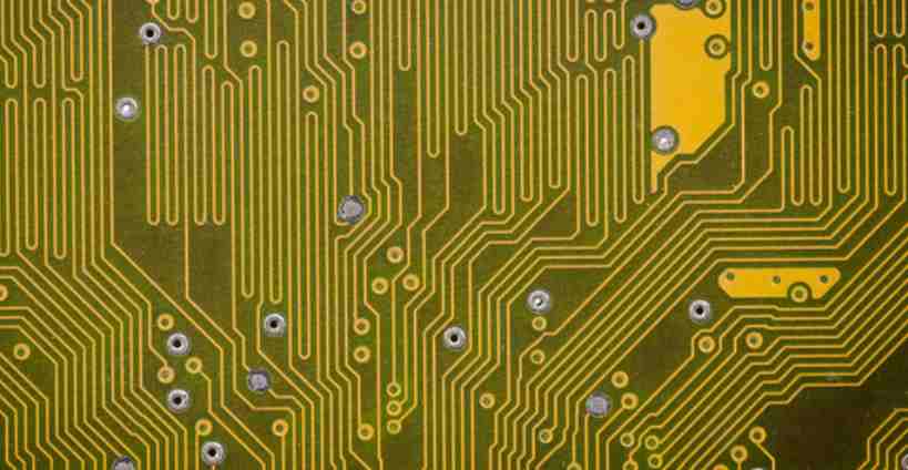
There are basically printed circuit boards inside electronic equipment, also known as printed circuit boards. The green circuit board, made of precious metal, connects all the electrical components of the device and allows it to function properly. Without PCBS, electronics will not work.
Ii. PCB schematic diagram and PCB design
A PCB schematic is a simple two-dimensional circuit design that shows the function and connectivity between different components. PCB design is a three-dimensional layout, in order to ensure the normal operation of the circuit after marking the location of the components.
Therefore, a PCB schematic is the first part of designing a printed circuit board. This is a graphical representation, whether written or in data form, that describes a circuit connection using an agreed upon symbol. It also suggests which components will be used and how they are wired.
As the name implies, a PCB schematic is a plan, a blueprint. It does not specify where the component will be placed specifically. Rather, the schematic lays out how the PCB will eventually achieve connectivity and forms a key part of the planning process.
After the blueprint is completed, the next step is the PCB design. A design is a layout or physical representation of a PCB schematic, including the layout of copper wiring and holes. The PCB design shows the location of the above components and their connection to the copper.
PCB design is the stage related to performance. Engineers built the actual components on top of the PCB design, allowing them to test whether the equipment was working properly. As we mentioned earlier, anyone should be able to understand the PCB schematic, but it's not easy to understand its function by looking at the prototype.
After both stages are complete and you are satisfied with the PCB's performance, you need to implement it through the manufacturer.
Three, PCB schematic elements
With a rough understanding of the differences between the two, let's take a closer look at the elements of the PCB schematic. As we mentioned, all connections are visible, but there are a few considerations to keep in mind:
In order to be able to see the connections clearly, they are not created to scale; In PCB design, they can be very close to each other
Some connections may cross each other, which is practically impossible
Some connections may be on opposite sides of the layout, with markers indicating that they are linked
This PCB "blueprint" can take one, two or even several pages to describe everything that needs to be included in the design
A final point to note is that more complex schematics can be grouped by function to improve readability. Arranging connections in this way will not happen in the next phase, and schematics often do not match the final design of the 3D model.
Four, PCB design elements
Now it's time to delve deeper into the elements of the PCB design document. At this stage, we move from written blueprints to physical representations constructed using laminate or ceramic materials. Some of the more complex applications require flexible PCBS when particularly compact Spaces are required.
The contents of the PCB design document follow the blueprints produced by the schematic process, but, as mentioned earlier, the two are very different in appearance. We've talked about the PCB schematics, but what differences can be observed in the design document?
When we talk about a PCB design document, we are talking about a 3D model that includes the printed circuit board and the design document. They can be single or multi-story, although two stories are most common. We can observe some differences between the PCB schematic and the PCB design document:
All components are correctly sized and positioned
If two points should not be connected, they must be detoured or switched to another PCB layer to avoid crossing each other on the same layer
In addition, as we discussed briefly, PCB design is more concerned with actual performance, as this is in some ways the verification phase of the final product. At this point, the practicality of the design must come into play, and the physical requirements of the printed circuit board must be considered. Some of them include:
How are the components spaced to allow adequate heat distribution

Edge connector
In terms of current and heat, how thick the tracks must be
Because physical limitations and requirements mean that PCB design documents often look very different from the designs on the schematic, the design documents include screen printing layers. The silk-screen layer indicates letters, numbers and symbols to help engineers assemble and use the board.
It is required to work as planned after all components are assembled on the printed circuit board. If not, you need to redraw.
Although PCB schematics and PCB design documents are often confused, actually making a PCB schematics and PCB design refer to two separate processes when creating a printed circuit board. The PCB schematic diagram that can be mapped must be created before the PCB design, which is an important part of determining the performance and integrity of the PCB.
Types and design standards of pad in PCB design
Feb 10,2023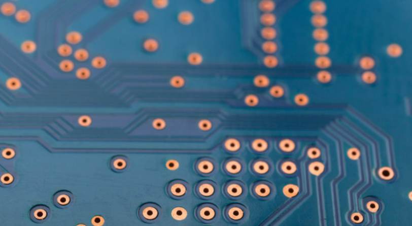


Just upload Gerber files, BOM files and design files, and the KINGFORD team will provide a complete quotation within 24h.