
Professional PCB manufacturing and assembly
Building 6, Zone 3, Yuekang Road,Bao'an District, Shenzhen, China
+86-13410863085Mon.-Sat.08:00-20:00

In the consultation of many customers, questions about PCB assembling board proofing are often asked. Of course, there are a lot of new customers for PCBA plate proofing is not very understanding. So, what are the benefits of PCB Mosaic proofing?
1. In order to improve the qualified rate of electronic products, it is necessary to ensure the quality of PCB, the core component, so it is necessary to produce a small amount of PCB samples in advance to test the performance of products, which can not only improve the production efficiency, but also reduce the production cost.
2, patchwork proofing is an effective measure to reduce production costs. PCB board for the whole PCBA processing process will be much less processes, a whole board, no matter 20 or 10, is to maximize the use of production resources, improve the efficiency of production.
3, PCBA plate proofing for the manufacturer's front-end engineering has great benefits. They can better participate in the production of customers' products, better understand the production and technological difficulties of customers' products; It is of great benefit to the subsequent production quality control. Such early participation helps to control production risks and improve customer satisfaction.
4. It can minimize the quality problems that may be encountered in mass production. After all, ensuring a good reputation is crucial for a manufacturer.

Why should pcb be assembled? For customers, pcb board is to facilitate plug-in; For pcb manufacturers, pcb assembling board is to improve the utilization rate of board and save production cost.
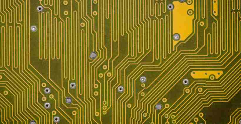
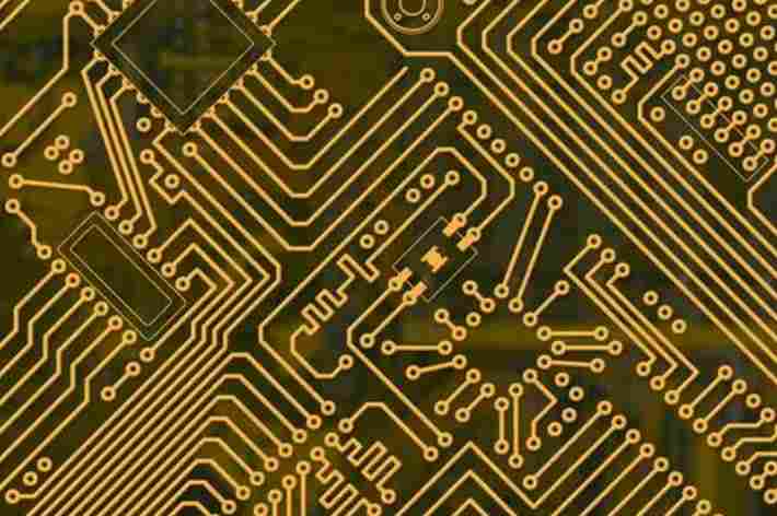
There are three types of pcb assembly: V-CUT, stamp hole and hollow joint. The following details and you explain:
PCB splicing mode -V cutting
V-CUT, also known as V-cut, is used more in the rule board. V cutting is to draw a slot at the connection of two boards, as long as the two boards are put together, leaving a gap between them (generally 0.4mm), but this place the connection of the board is relatively thin, easy to break, when the board needs to combine the edges of the two boards together. V cuts are generally straight lines, without complex lines such as curved arcs. When assembling plates, they should be on a straight line as far as possible. V secant lines can be represented by 2D lines placed on all layers.
PCB Mosaic mode - Stamp hole
For irregular PCB board, such as circular, V cutting is not possible, at this time, it is necessary to use the stamp hole to make the plate connection, so the stamp hole is generally used more in the special-shaped board. The edges of the two boards are connected by a small piece of board, and the small piece of board has many holes where the two boards join, which is easy to break. When broken off, the edges of the board look like the edges of a stamp, so this arrangement is called a stamp hole.
PCB Mosaic mode - hollow connection strip
The hollow connection bar is used more in the board with a half hole process. It is the use of a very narrow plate to connect, which is similar to the stamp hole. The difference is that the connection part of the connection bar is a little narrower, and there is no hole on both sides. There is one disadvantage of the splicing method of the hollow joint: the splicing will have a very obvious convex point. Stamp holes also have raised spots, which are less noticeable because they are separated by the holes. One might think that why use a hollow connection bar instead of a stamp hole? This is because when the module is surrounded by half holes, stamp holes and V cuts can not be used, and can only be connected through hollow connecting strips at the four corners of the module.
Check the process after pcb wiring is completed
After the PCB routing design is completed, it does not mean that it has been successful. In order to make the PCB operate better and have better quality, it is usually necessary to check whether the PCB routing design conforms to the rules.
Whether the established rules do not meet the requirements of PCB production process. How to check after PCB wiring? Let's look at the PCB wiring inspection method.
1. Check whether the distance between the through holes is reasonable.
2. Check whether the width of the power cable and ground cable is appropriate.
3. Check whether the best measures are taken for key signal cables.
4. Check whether the analog circuit and the digital circuit have independent ground cables.
5. Check whether the graphics added to the PCB cause signal short circuit.
6. Check whether there are process lines on the PCB.
7. Check whether the edge of the outer frame of the power layer on the multi-layer PCB board is narrowed.


Just upload Gerber files, BOM files and design files, and the KINGFORD team will provide a complete quotation within 24h.