
Professional PCB manufacturing and assembly
Building 6, Zone 3, Yuekang Road,Bao'an District, Shenzhen, China
+86-13410863085Mon.-Sat.08:00-20:00

In PCB proofing, how to reduce or eliminate the deformation caused by different material characteristics or processing has become one of the most complicated problems faced by PCB manufacturers. Below, let the engineer share with you: What are the causes of PCB board deformation?
1, the weight of the circuit board itself will cause the board sag deformation
Generally, the back welding furnace will use the chain to drive the circuit board forward in the back welding furnace. If there are too heavy parts on the board, or the size of the board is too large, it will show the middle depression phenomenon because of its weight, resulting in the bending of the plate.
2. The depth of V-Cut and the connecting strip will affect the deformation of the plate
V-Cut is to cut grooves on the original large sheet, so the place where V-Cut occurs is prone to deformation.
3. Deformation caused by PCB board processing
The deformation causes of PCB board processing are very complex, which can be divided into thermal stress and mechanical stress. The thermal stress is mainly produced in the process of pressing, and the mechanical stress is mainly produced in the process of stacking, handling and baking. The following is a brief discussion in process order.
Incoming materials of copper clad plate: the size of the copper clad plate press is large, and the temperature difference between different areas of the hot plate will lead to slight differences in the curing speed and degree of the resin in different areas during the pressing process, and also produce local stress, which will gradually release and produce deformation in the future processing.
Pressing: PCB pressing process is the main process of generating thermal stress, which is released in the subsequent drilling, shaping or barbecue process, resulting in the deformation of the plate.
Welding resistance, character baking process: because the welding resistance ink curing can not stack each other, so PCB board will be vertically placed in the shelf drying board curing, the board is easy to deformation under the weight or oven strong wind.
Hot-air solder leveling: The whole hot-air solder leveling process is a sudden heating and cooling process, thermal stress will inevitably occur, resulting in microscopic strain and overall deformation warping zone.
Storage: PCB board in the semi-finished product stage is generally firmly inserted in the shelf, the shelf tightness adjustment is not appropriate, or in the storage process of stacking board will cause mechanical deformation of the board.
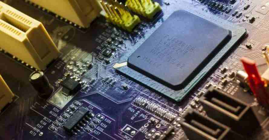
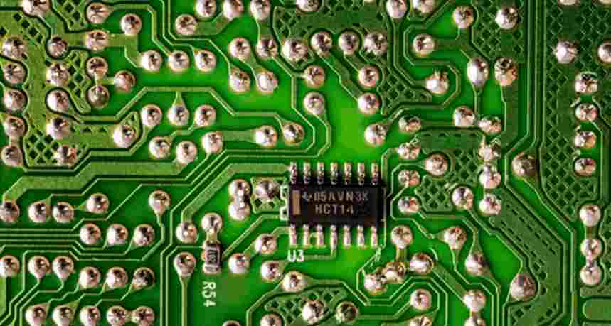
PCB is the core component of electronic products, known as the "mother of electronic components", widely used in various fields. So, what are the advantages of PCB board?

1. Maintainability. Because PCB products and components assembly components are based on standardized design and large-scale production; Therefore, these components have normative rationality. In case of failure, it can be replaced efficiently, quickly, conveniently and flexibly, and the system can be restored quickly.
2. Improve stability. Through a series of checks, inspections and aging tests, the PCB can be guaranteed to work reliably for a long time.
3. Assemblability. It is convenient for standardized assembly, and can be automated and large-scale batch production. At the same time, PCB and each component assembly parts can also be assembled into larger parts, systems, until the whole machine.
4. Be productive. Adopt modern management, can carry out standardization, scale, automation and other production, to ensure the consistency of product quality.
5. Designability. PCB performance (electrical, physical, chemical, mechanical, etc.) requirements, can be achieved through design standardization, standardization, etc.
6, can be high-density. With the integration of integrated circuit and installation technology progress and development.
7. Testability. Establish complete inspection methods, inspection standards, and all kinds of inspection equipment and instruments, etc., to test and evaluate the qualification and service life of PCB sample products.
8, other: such as the system miniaturization, slight, high-speed signal transmission, etc.
PCBA processing quotation and PCBA processing process
PCBA processing quotation mainly involves PCB board fee, component purchase fee and welding processing fee three parts. Chengdu Zicheng Electronic is professional to provide PCBA electronic manufacturing services professional manufacturers, share with you the process of PCBA quotation method.
PCBA processing quotation steps are roughly divided into the following steps
1. Calculate the total material cost according to BOM and Gerber documents;
2. Calculated the cost of SMT patch and DIP plug-in processing;
3. Calculate the cost of PCBA testing (such as ICT, FCT testing, etc.);
4. Packaging logistics evaluation.
According to the customer's region and product characteristics, cost addition pricing is generally adopted, that is, in the quotation = cost *(1+x%), where x needs the above comprehensive evaluation, according to experience, x% is generally within this range: ≤20%.
PCBA processing quotation needs to be provided
1. Complete PCB board making files (Gerber files, positioning maps, steel mesh files) and board making requirements;
2. Complete a BOM(including the model, brand, package, and description).
3. PCBA assembly drawing.
PS: Report the PCBA function test fee, and provide the PCBA function test method.
1. Customers place orders
Customers place orders according to their actual needs of PCBA processing plants, and put forward specific requirements. The processing plant will evaluate its capacity to see if it can fulfill the order. If the manufacturer is sure that they can complete the order within the expected time, then the two parties will negotiate to determine the production details.
2. Production materials provided by customers
After the customer decides to place an order, he shall provide a series of documents and lists to the PCBA processing plant, such as PCB electronic files, coordinate files, BOM list and so on, which must be provided.
3. Purchase raw materials
PCBA processing plant purchases relevant raw materials from designated suppliers according to the documents provided by customers.
4. Incoming material inspection
Before PCBA processing, strict quality inspection is carried out for all raw materials to be used to ensure that they are qualified before being put into production.
5. PCBA production
In the process of PCBA processing, in order to ensure the quality of production, whether it is patch or welding production, the manufacturer needs to strictly control the furnace temperature.
6. PCBA test
The PCBA processing plant conducts rigorous product testing, and the PCB board that passes the test is delivered to the customer.
7. Packaging after sale
After the PCBA processing is completed, the products are packaged and then handed over to the customer to complete the whole PCBA processing.
What are the advantages of PCB Mosaic proofing?
Feb 10,2023


Just upload Gerber files, BOM files and design files, and the KINGFORD team will provide a complete quotation within 24h.