
Professional PCB manufacturing and assembly
Building 6, Zone 3, Yuekang Road,Bao'an District, Shenzhen, China
+86-13410863085Mon.-Sat.08:00-20:00

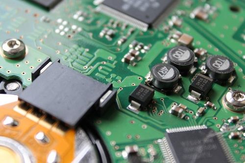
PCB board is composed of copper foil, resin, glass cloth and other materials, the physical and chemical properties of each material are different, after pressing together will inevitably produce thermal stress residual, resulting in deformation. At the same time, in the process of PCB processing, it will go through various processes such as high temperature, mechanical cutting and wet treatment, which will also have an important impact on the deformation of the board. In short, the causes of PCB board deformation are complex and diverse. How to reduce or eliminate the deformation caused by different material characteristics or processing has become one of the most complex problems faced by PCB manufacturers.
Cause analysis of deformation
The deformation of PCB board needs to be studied from several aspects, such as material, structure, graphic distribution, processing process, etc. This paper will analyze and elaborate various causes of deformation and improvement methods. The copper surface area on the circuit board is uneven, which will worsen the bending and warping of the board.
Generally, a large area of copper foil will be designed on the circuit board for grounding. Sometimes, Vcc layer will also be designed with a large area of copper foil. When these large areas of copper foil are not evenly distributed on the same circuit board, it will cause the problem of uneven heat absorption and heat dissipation speed. If the expansion and contraction cannot be done at the same time, it will cause deformation under different stresses. At this time, if the temperature of the board has reached the upper limit of Tg value, the board will begin to soften, resulting in permanent deformation.
The connections between the layers on the board limit the board's growth and shrinkage. Most of today's circuit boards are multilayer boards, and there will be rivets between layers of connection points, and the connecting points are divided into through holes, blind holes and buried holes, where the connecting points will limit the effect of the board, but also indirectly cause the bending and bending of the board.
The weight of the board itself can cause the board to sag and deform. General back welding furnace will use the chain to drive the circuit board forward in the back welding furnace, that is, to both sides of the board when the fulcrum to prop up the whole board, if the board above the excess parts, or the size of the board is too large, it will be due to its own kind of amount and show the middle depression phenomenon, resulting in bending.
The depth of V-Cut and the connection strip will affect the deformation of the plate. Basically, V-Cut is the culprit of damaging the structure of the board, because V-Cut is in the original a large sheet of the board to cut out grooves, so the V-Cut place is prone to deformation.
Noise analysis of sheet deformation caused by compacted materials, structures and graphics
PCB board is made of core board, semi-cured sheet and outer copper foil pressed together. The core board and copper foil are deformed by heat when pressed together. The deformation depends on the coefficient of thermal expansion (CTE) of the two materials. The coefficient of thermal expansion (CTE) of copper foil is about. The common FR-4 substrate is z-oriented to CTE below the Tg point. Above TG point is (250~350)X10-6, and x-direction CTE is generally similar to copper foil due to the existence of glass cloth.

A note on TG points:
When the temperature of high Tg printed board rises to a certain area, the substrate will change from glass state to rubber state, and the temperature at this time is called the glass transition temperature (Tg) of the board. That is, Tg is the highest temperature (° C) at which the substrate remains rigid. That is to say, ordinary PCB substrate materials at high temperature, not only produce softening, deformation, melting and other phenomena, but also show a sharp decline in mechanical and electrical characteristics. The plate of general Tg is more than 130 degrees, the high Tg is generally more than 170 degrees, and the medium Tg is about more than 150 degrees. Usually Tg≥170℃ PCB printed board, called high Tg printed board.
With the increase of Tg of the substrate, the characteristics of heat resistance, moisture resistance, chemical resistance and stability of the printed board will be enhanced and improved. The higher the TG value, the better the temperature resistance of the plate, especially in the lead-free process, high Tg is often used. Among them, the expansion of the core plate that makes the inner pattern is different due to the difference between the pattern distribution and the thickness of the core plate or the material characteristics. When the pattern distribution is different from the thickness of the core plate or the material characteristics, the pattern distribution is uniform and the material type is consistent, there will be no deformation. When the PCB lamination structure is asymmetrical or the pattern distribution is not uniform, the CTE difference of different core boards will be large, resulting in deformation in the process of pressing.
Deformation caused by PCB board processing
The deformation causes of PCB board processing are very complex and can be divided into thermal stress and mechanical stress. The thermal stress is mainly produced in the process of pressing, and the mechanical stress is mainly produced in the process of stacking, handling and baking.
Incoming materials of copper clad plate: All copper clad plates are double panels, symmetrical structure, no graphics, copper foil and glass cloth CTE are almost the same, so in the process of pressing almost no deformation caused by different Ctes. However, the large size of the copper clad plate press and the temperature difference in different areas of the hot plate will lead to slight differences in the curing speed and degree of the resin in different areas during the pressing process. Meanwhile, the dynamic viscosity under different heating rates is also very different, so the local stress caused by the difference in the curing process will also be generated. Generally, the stress will maintain balance after pressing, but will gradually release and produce deformation in the future processing.
Pressing: The pressing process of PCB is the main process of generating thermal stress. The deformation caused by different materials or structures is analyzed in the previous section. Similar to the pressing of copper clad plate, local stress caused by the difference in curing process will also be generated. The thermal stress of PCB board will be more difficult to eliminate than that of copper clad plate due to thicker thickness, diversified pattern distribution, more semi-cured sheets and other reasons. The stress in the PCB board is released in the process of drilling, shaping or barbecuing, resulting in the deformation of the board.
Welding resistance, character baking process, etc. : Since the welding resistance inks cannot be stacked when curing, PCB boards will be placed vertically on the shelf for drying board curing. The welding resistance temperature is about 150℃, which is just above the Tg point of medium and low Tg materials.
Hot air solder leveling: ordinary plate hot air solder leveling temperature of tin furnace is 225℃~265℃, the time is 3S-6S. The hot air temperature is 280℃~300℃. The solder is processed into the tin furnace from room temperature, and the post-treatment water is washed at room temperature within two minutes after it comes out. The whole hot-air solder leveling process is sudden heating and sudden cooling process. Due to the different materials and uneven structure of the circuit board, thermal stress will inevitably occur in the process of cooling and heating, resulting in microscopic strain and overall deformation warped zone.
Storage: PCB board in the semi-finished product stage is generally firmly inserted in the shelf, the shelf tightness adjustment is not appropriate, or in the storage process of stacking board will cause mechanical deformation of the board. Especially for the thin plate less than 2.0mm, the impact is more serious.
How can we prevent the bending and warping of the plate after the back welding furnace?
1. Reduce the influence of temperature on the stress of the plate
Since the temperature is the main source of the stress of the plate, as long as reducing the temperature of the backwelding furnace or slowing down the heating and cooling speed of the plate in the backwelding furnace, the bending and warping of the plate can be greatly reduced. But there may be other side effects.
2. High Tg plate is used
Tg is the glass conversion temperature, that is, the temperature at which the material changes from glass state to rubber state. The lower the Tg value is, the faster the board will become soft after entering the backwelding furnace, and the longer it will take to become soft rubber state, the more serious the deformation of the board will be. The plate with higher Tg can increase its ability to withstand stress and deformation, but the price of the material is relatively high.
3. Increase the thickness of the circuit board
Many electronic products in order to achieve the purpose of thinner, the thickness of the board has been left 1.0mm, 0.8mm, and even made to 0.6mm thickness, it is recommended that if there is no light and thin requirements, the board can best use the thickness of 1.6mm, can greatly reduce the risk of bending and deformation of the board.
4. Reduce the size of the circuit board and reduce the number of boards
Since most backwelding furnaces use chains to drive the circuit board forward, the larger the size of the circuit board will sag and deform in the backwelding furnace because of its own weight, so try to put the long side of the circuit board as the board side on the chain of the backwelding furnace, you can reduce the weight of the circuit board caused by the sag deformation, reduce the number of plates is also based on this reason, That is to say, when the furnace, as far as possible to use the narrow side of the vertical direction of the furnace, can achieve the lowest depression deformation.
5. Use real connection and stamp hole instead of V-Cut sub-board
Since V-cuts can damage the structural strength of the board, try not to use V-Cut subboards, or reduce the depth of the V-Cut.
In addition to the production process, the storage of PCB board parts at each station also has a certain impact on the deformation. In some manufacturers, due to more production waiting and narrow site, multiple boards will be stacked together for storage, which will also lead to external deformation of the board parts. Since PCB board also has a certain plasticity, these deformation will not be 100% recovered in the later flattening process. Most PCB manufacturers will have a leveling process before shipment. This is because the deformation of the plate caused by heat or mechanical force is inevitable in the processing process, which can be effectively improved by mechanical leveling or hot drying leveling before shipment.
PCB copying board cleaning technology
Feb 10,2023


Just upload Gerber files, BOM files and design files, and the KINGFORD team will provide a complete quotation within 24h.