
Professional PCB manufacturing and assembly
Building 6, Zone 3, Yuekang Road,Bao'an District, Shenzhen, China
+86-13410863085Mon.-Sat.08:00-20:00

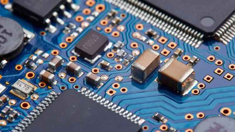
A Blind via is a through-hole that connects the inner layer to the outer layer. The Buried via is a blind hole that connects the inner layer to the inner layer. They are all small holes with a diameter of 0.05mm~0.15mm. The hole forming methods of buried blind holes include laser forming, plasma etching and photoforming. Laser forming is usually used, and the laser forming is divided into CO2 and YAG ultraviolet laser machine (UV). Traditional PCB board drilling due to the impact of drilling tool, when the hole diameter reaches 0.15mm, the cost is already very high, and it is difficult to improve again. The drilling of HDI board no longer relies on traditional mechanical drilling, but uses laser drilling technology. (So it is sometimes called laser plate) the hole diameter of the HDI board is generally 3-5mil (0.076-0.127mm), the line width is generally 3-4mil (0.076-0.10mm), the size of the pad can be greatly reduced so the unit area can get more line distribution, high-density interconnection from this. Then what are the causes of blind hole interconnection failure of the HDI board?
The difference of material growth and shrinkage is too large
Material matching also plays an important role in the reliability of blind hole interconnection. Secondary laminate L1-L2 is made of RCC material, and L2-L3 electroplating blind hole filling layer is made of LDP material. Because the circuit board in lead-free welding under the influence of high temperature and heat, the blind hole filling, LDP and RCC materials with different Ctes in electroplating have different degrees of expansion and shrinkage, which makes the proportion of blind hole ICD in LDP layer increase obviously. Therefore, attention should be paid to the selection of materials and the matching of materials when making multiple laminates.
Halogen-free RCCS increase the incidence of blind hole ICDs
Halogen-free RCC material is a new material developed according to the requirements of RoHS directive. It does not contain halogen prohibited by RoHS but also has excellent fire resistance. The main resistance mechanism is to replace the halogen with P and N, which reduces the polarity of the polymer chain and increases the molecular weight of the resin. At the same time, the addition of filler such as aluminum oxide also increases the polarity of the material, so that the halogen-free material shows some different characteristics from the conventional epoxy resin. Therefore, there will be some problems in combining halogen-free materials with the original electroplating potion four, and thin plating may occur.
The energy of laser hole etching is too large
Laser hole etching method is the main production process of blind hole production at present. Although CO2 laser can not directly ablate the copper layer, if the copper layer is specially treated to make its surface have strong infrared wavelength absorption characteristics, the copper layer will quickly rise to a very high temperature in an instant. The inner copper at the bottom of the blind hole is generally browned. Because the surface of the browned copper reflects less laser, and its rough surface structure increases the diffuse reflection of light, thus increasing the absorption of light waves, and the surface of the browned copper box is an organic layer structure, which can also promote the absorption of light. Therefore, if the laser energy is too large after laser drilling, it is possible to recrystallize the inner copper surface layer at the bottom of the blind hole, resulting in changes in the inner copper structure.
It is not clean to remove glue residue
It is a very important process before blind hole electroplating. It plays a very important role in the reliability of the connection between the copper in the hole wall and the copper in the inner layer. Because a thin resin layer may leave the blind hole in a semi-conductive state. During the E-TEST test, due to the pressure effect of the needle, the test may be passed, and after the plate assembly, open circuit or contact failure may occur. However, taking mobile phone plate as an example, there are about 7~ 100 thousand blind holes on each plate, and it is inevitable that there will be occasional mistakes when removing glue. Due to the current manufacturers of the erosion potion system has been very perfect, so only close monitoring of the tank, before it is about to go wrong, make a quick decision to replace the tank to ensure the due yield.
The copper plating on the inner connecting disk is abnormal
The abnormal quality of the copper plating layer on the surface of the inner connecting disk is also one of the reasons for the blind hole interconnection failure, because the physical properties of the copper plating layer, such as ductility, tensile strength, internal stress and compactness, play an important role in the reliability of the blind hole, and the physical properties of the copper plating layer depend on the organizational structure and chemical composition of the copper layer. Blind hole bottom inner connecting plate surface coating rough caused by interconnection failure, such inner copper surface, one is easy to lead to the removal of rubber unclean, three is due to the crystallization of the copper surface itself, blind hole electroplating is prone to chemical precipitation copper and inner copper bonding force is poor and other defects, so once the tensile stress is very easy to send interconnection failure.
Excessive heat or rework times of manual welding
During the assembly of HDI board parts, manual welding is also required in some positions. The temperature of manual welding, the proficiency level of welding personnel during operation and the number of rework will greatly affect the welding quality.


Just upload Gerber files, BOM files and design files, and the KINGFORD team will provide a complete quotation within 24h.