
Professional PCB manufacturing and assembly
Building 6, Zone 3, Yuekang Road,Bao'an District, Shenzhen, China
+86-13410863085Mon.-Sat.08:00-20:00

High voltage design of PCB design line
Copper is a strong conductor with a high melting point, but you should still try to keep it cold. Here, you need to adjust the size of the wire width to keep the temperature within a certain range. However, this is where you need to consider the current flowing in a given path. When using power rails, high voltage components, and other heat sensitive parts of the board, the PCB line width in relation to the ammeter can be used to determine the line width to use in the layout.
One problem with most tables is that they do not solve the controlled impedance routing problem. You have determined the size of the line in order to control the impedance, * it is difficult to determine the temperature rise by looking at the table, and you must use a calculator. However, an alternative method is to use the IPC 2152 Normogram to check that the current-temperature relationship is within the operating range of the controlled impedance curve.
In my day job, I find myself spending a lot of time browsing EE forums. A problem that often arises during PCB design and wiring is determining the recommended wiring widths to keep the temperature of the device within a certain range of a given current value, and vice versa. Although copper has a high melting point and can withstand high temperatures, you should ideally keep the board's temperature rise to less than 10°C. Allowing PCB wiring to reach very high temperatures increases the ambient temperature seen by the component, which puts a greater burden on active heat dissipation measures. Model the received EMI in PCB design. Hefei multi-layer PCB design and development scheme
Schematic design is an important part of PCB design, design a satisfactory circuit must be drawn schematic circuit.
The general design process of schematic diagram is as follows:
New schematic -- set drawing -- load schematic library (no need to build yourself)-- place the original -- adjust the original -- wire -- add other electrical symbols -- check and modify -- export grid table.

Basic principles of circuit schematic design:
1. The components are placed according to the principle of modularization and signal, so that the designed schematic diagram is convenient for circuit function and principle analysis.
2, the components in the same module as close as possible, different modules slightly away from the components.
3, do not have too many cross lines, too far parallel lines. Make full use of electrical symbols such as bus, network label and circuit port to make schematic diagram clear.
PCB design automatic wiring and automatic interactive wiring.
Grounding serves three important purposes on PCB boards:
1. Voltage return: Most of each component on the PCB will be connected to the power network, and then the return voltage will be returned via the ground network. On boards with only one or two layers, the grounding network must usually be routed using a wider route. However, the process of connecting each component to the grounding grid can be simplified by integrating the entire layer into the grounding layer of the multilayer board.
2, signal return: conventional signals also need to return, for high-speed design, it is very important to have a clear return path on the ground. Without this clear return path, these signals can be very disruptive to the rest of the PCB.
3, reduce noise and interference: with the increase of signal speed, digital circuit switching state will be more and more. This produces noise pulses through the grounding circuit, which may affect other parts of the circuit. A grounding layer with a larger conducting area helps to reduce this interference because it has a lower impedance than grounding grids do through wire routing.
By carefully planning the layer-stack configuration of multilayer boards, PCB designers can use layer-bonding to help control the electrical performance of the boards. By using ground layers between two active signal layers, crosstalk between signals on these layers can be eliminated. And the signal integrity of high-speed transmission lines can be improved by ensuring that there is an uninterrupted signal return path on the ground surface. The ground layer is also usually attached to the heated component to help dissipate heat.
PCB design line inductance and width Not all design rules apply in every case and are often communicated without context. A special rule for resizing a trace is to always choose a wider trace whenever possible. Unlike many rules of thumb I've seen, this particular rule has certain advantages. However, when you need to control the line impedance and reduce ringing at the same time, you need to carefully control the line width to ensure that the transmission line has the required impedance within a specific tolerance. Let's look at the basic formula for adjusting the stitch size and how to keep the impedance within the tolerance. Similar equations have been developed for symmetric strip lines, embedded microstrip lines, coplanar waveguides, and offset/asymmetric strip lines. For now, I'll limit the discussion to microstrips, but you can follow the other trace geometry outlined here. What is your schematic netsheet for your PCB? .
How is the chip welded to the circuit board?
Feb 08,2023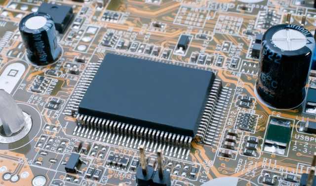


Just upload Gerber files, BOM files and design files, and the KINGFORD team will provide a complete quotation within 24h.