
Professional PCB manufacturing and assembly
Building 6, Zone 3, Yuekang Road,Bao'an District, Shenzhen, China
+86-13410863085Mon.-Sat.08:00-20:00

With the continuous development of manufacturing and electronic technology, the function of hardware circuit system is becoming more and more powerful, the circuit composition is becoming more and more simple, and the importance of software function is gradually increasing, but the importance of PCB design is also very important. No matter how perfect the system software is developed, if the hardware PCB design is not reasonable, the system performance will be greatly reduced, there will be serious power consumption, equipment restart, or even can not work. Hardware PCB design is generally divided into design requirements analysis, schematic design, PCB design, process document processing, sample testing and other stages. Hardware circuit design has mature methods and basic principles, in the design process there are also some matters needing attention. Only under the framework of following the basic principles and precautions can we develop the hardware circuit with perfect performance and stability, which provides the foundation for realizing the software function. We have several hardware engineers working for 10 years, to provide you with professional PCB design services. PCB designers should minimize the number of bypass capacitors, which can increase current loss. Hefei simple PCB design wiring
Factors affecting PCB solder joint strength
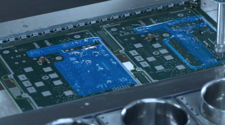
To solder components onto the PCB, the circuit board will have to undergo a manual or automatic welding process. It is important here to understand the factors that affect PCB solder joint strength.
Some of these factors are related to your layout, while others are related to the welding process itself. The two are actually related, and a few simple design choices can help ensure that your solder joints are strong, that components are not damaged during reflow soldering, and that there are no accidental Bridges. A lot of manual rework can seriously prolong your delivery time, but using the right CM will help ensure that your design does not encounter common problems that can affect PCB solder joint strength.
1, solder quality: temperature distribution, wetting and flux
2. Flux and oxidation
3. Temperature and wetting
4, whether you should use heat sink to enhance PCB solder joint strength?
5. Damage
6, PCB design wiring PCB design rules to improve productivity and profit.
PCB design parasitic resistors, inductors and capacitors
Many designers are used to thinking about system behavior in terms of circuit models. These models and circuit diagrams are all correct to some extent, but they are missing some important information to determine the behavior of the system. The missing information in the circuit diagram is the geometry of the actual PCB layout, which determines how the elements in the system are electrically and magnetically coupled to each other.

So what causes electromagnetic coupling between circuit components, conductors, ferrites, and other complex structures in a real PCB or IC? This is determined by the interaction between electromagnetic fields and matter, but the conceptual way to summarize signal behavior in complex systems is to think of coupling in terms of parasitic circuit elements or parasitism for short. Introducing parasitic effects into circuit models can help you explain unexpected or undesired signal and power behavior in real systems, making parasitic modeling tools very helpful for understanding circuit and product behavior.
This is because the circuit diagram simply cannot account for some important function of the actual PCB, IC or any other electrical system. Parasites are represented in the circuit diagram as resistors, capacitors, and inductors, depending on their behavior in the frequency domain. Note that parasitism is discussed almost entirely in terms of LTI circuits, which means that parasitism is also viewed as linear and time-dependent. Time-varying and nonlinear parasites employ more sophisticated modeling techniques, which involve manual iteration in the time domain. They can also be very sensitive to the initial conditions of the system, especially in the presence of feedback.
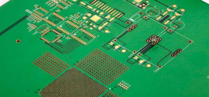
How to judge the quality of PCB design has the following points: 1, size and thickness of the standard rules. Customers can measure and check their own product thickness and specifications. 2. Light and color. External circuit boards are covered with ink, circuit boards can play the role of insulation, if the color of the board is not bright less ink, then PCB itself is not good. 3. Appearance of weld. There are many PCB parts. If the welding is not good, the parts will fall off easily, which will seriously affect the welding quality. 4. After the installation of components, the telephone should be easy to use, that is, the electrical connection should meet the requirements.
5, line width, line thickness, line distance meet the requirements, so as to avoid line heating, open circuit, and short circuit. 6, by high temperature copper is not easy to fall off. 7, copper surface is not easy to oxidize, affect the installation speed, oxidation after use soon after bad. 8. No additional electromagnetic radiation. 9. The shape is not deformed, so as to avoid the deformation of the shell and dislocation of the screw hole after installation. Now the installation is mechanized, the hole location of the circuit board and the deformation error of the circuit and the design should be within the allowable range. 10. High temperature, high humidity and special environment should also be considered. 11. The mechanical properties of the surface should meet the installation requirements. Assembly type PCB component placement accuracy requirements.


Just upload Gerber files, BOM files and design files, and the KINGFORD team will provide a complete quotation within 24h.