
Professional PCB manufacturing and assembly
Building 6, Zone 3, Yuekang Road,Bao'an District, Shenzhen, China
+86-13410863085Mon.-Sat.08:00-20:00

Printed circuit board design is a skill that can help you make your own electronics, whether as a professional or an amateur. In the professional field of electronic engineering, one can find PCBS in any electronic equipment, such as: mobile phone chargers, toys, washing machines, etc.
In this article, you will be able to learn how to design your own professional PCB board (including schematics, PCB layout, gerber generation and 3D models). We will provide you with the best tips and tricks, including free software that will help you improve your skills from beginner to expert level in PCB layout design and electronics. We will cover the following topics:
Top 10 PCB design software in 2020
Component packaging selection and arrangement
Top 10 Wiring tips for PCB Layout
Six basic design rules for any PCB design
Single-layer and multi-layer PCB design
Printed circuit board shape and size
Patch with through hole
3D view of the project /CPL file
Design the circuit board of smartwatch
Nine PCB design software: Below are nine professional PCB design software that can be used to design any type of printed circuit board. Some of the software is free to download and use.
Component package selection
After using one of the above software design schematic or circuit diagram. You need to test the ERC (Electrical Rule Check), which will help you verify the joints and connections in the design schematic.
After successful ERC testing, the next step is to select a suitable package for the PCB board. After selecting the right package for your components, the next step is to arrange and rotate each component in a specific position. When arranging the components, keep in mind the utility circuit board, which you want to treat as a final product.
Top 10 PCB design and wiring tips
In electronic design, wiring, often referred to simply as "wiring," is a step in the design of a printed circuit board (PCB). It builds on the previous step, called placement, which determines the location of each active component of the IC or component on the PCB. Here are the first 10 steps for PCB design and wiring:
1. Always create a ground plane
2. Heat dissipation through holes
3. Don't rely on your automatic router - be sure to check critical networks with your own eyes
4. Know the manufacturer's specifications - Follow each vendor's layout recommendations
5. Figure out your line width-contact your PCB manufacturer for their design rules
6. Leave plenty of space between wiring -- check with your PCB manufacturer for their design rules
7. Use capture grids to make your job easier
8. Avoid 90-degree line angles
9. Leave a space between the cable and the mounting hole
10. Make your power and ground cables wider
6 Basic Design Rules for any PCB design: All of our PCB designs have logical and physical aspects that need to be managed properly to create a perfect design, so what do the design rules do.
They allow you to define a system so that you can check these requirements automatically and provide you with an interface between the logical and physical sides. When you actually have the rules to define the requirements, you will be able to automatically perform DFM checks and ensure that you have a board that can be manufactured.

1. Polygon connection style
2. Solder resistance layer extension
3. Route through-hole style
4. Component gaps
5. Electrical clearance
6. Wiring width
Single-layer vs. multi-layer PCB design: Double-sided and single-sided PCBS are essentially the same. The difference is that the single panel has copper on one side of the panel. The single panel is also not technically copper plated in the borehole. Multilayer PCBS have more than two layers.
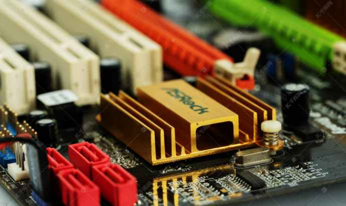
Patch and through-hole: Through-hole installation is the process of placing component leads into a borehole on a bare PCB. SMT components are secured to the board surface by solder only, while through-hole component leads are threaded through the board, allowing the components to withstand more ambient pressure.
Printed board shapes and sizes: It's not uncommon to see circles, triangles, or other interesting PCB shapes. Most PCBS are designed to be as small as possible, but not necessary if your application does not require it. If you plan to put the PCB into the housing, the size may be limited by the housing size. In this case, you need to know the dimensions of the housing before laying out the PCB so that everything fits inside.
The components you use will also have an impact on the size of the finished PCB. For example, surface mount components are small and flat in shape, so you will be able to make PCBS smaller. Through-hole components are larger, but generally easier to find and solder.
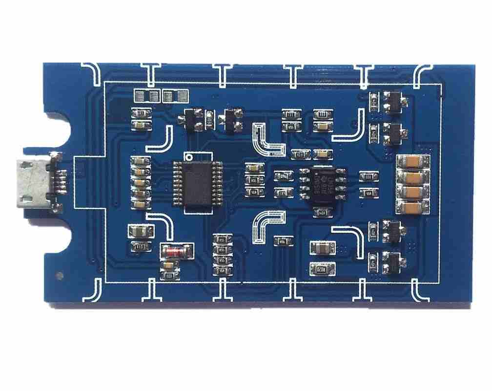
Generate Gerber files: The Gerber format is an open 2D vector image file format. It is the standard document used by printed circuit board (PCB) industry software to describe printed circuit board images. The Gerber file is required to manufacture and assemble the final PCB board. It contains the following aspects.
3D view of the project: Electronic projects look great in 3D view. We can see the final PCB design top, bottom, left, right, at specific angles. Here are some examples of 3D PCB boards.


Just upload Gerber files, BOM files and design files, and the KINGFORD team will provide a complete quotation within 24h.