
Professional PCB manufacturing and assembly
Building 6, Zone 3, Yuekang Road,Bao'an District, Shenzhen, China
+86-13410863085Mon.-Sat.08:00-20:00

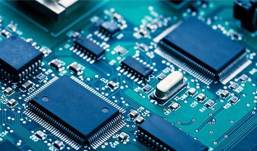
The birth and development of FPC and PCB board gave birth to the new product of the combination of soft and hard board. Therefore, the combination of soft and hard board, is the flexible circuit board and hard circuit board, after pressing and other processes, according to the relevant process requirements combined together, the formation of a circuit board with FPC characteristics and PCB characteristics.
FPC soft board after the completion of production, to go through what process to complete the production of hard and soft board.
1. Punch holes. Drill holes on the FR4 circuit board and PP film, and the design on the matching hole is not the same as the general through hole. After punching is completed, brown processing is required.

2. Riveting. The copper clad plate, PP glue, FPC circuit board are stacked and placed neatly. The original old process is stacked step by step production and pressing, but it is a waste of time. After many attempts, it is found that a stacking process can be completed.
3. Laminate. This is a relatively complete step in the production of soft and hard composite board. Most of the materials are integrated for the first time. First, the bottom layer of copper coated plate and PP film are integrated, and above is the FPC soft board made in the previous process. All materials to be laminated are placed in order to be pressed together.
4. Edge of gong plate (also known as edge removal). That is, the PCB board edge position does not have a line and will not make a line in the future part of the clear. Later, it is necessary to measure whether the material has excessive growth and shrinkage. Because the PI used in the production of soft board is also swollen and shrinkage, it has a great impact on the production of the circuit board.
5. Drill holes. This step is the first step of a step in which the entire PCB circuit board is switched on. The production parameters should be made according to the design parameters.
6. Remove glue residue. Plasma treatment will first PCB board drilling produced by the rubber slag removed, in the use of plasma cleaning will be through the hole and clean up the surface.
7. Sinking copper. This step is the process of electroplating through holes, also known as hole metallization. Realize through hole power conduction.
8.PCB board surface plating. Local electroplating copper is carried out on the surface above the electroplating hole so that the thickness of copper above the through hole exceeds a certain height of the copper-covered plate surface.
9. Outer dry film positive film production. The line to be etched on the copper-covered plate is produced in the same process as the anticorrosive dry film for the FPC soft plate. Line check after development.
10. Graphic plating. After initial copper deposition, graphic plating is carried out. Current time and copper plating wire are used according to design requirements to reach a certain plating area.
11. Alkaline etching

12. Seal resistance welding. This step has the same effect as the soft board protective film. We see that the hard board of PCB is usually green. It is this step, also known as printing green oil, that will be checked after the printing is completed. Customers also require other solder resistance inks, such as: butter, blue oil, red oil, white oil, black oil, photosensitive and matte.
13. Open the gong. Gong open cover is also called open cover, is the area where the soft plate is, but the hard plate does not need to be laser cut, so that the soft plate is exposed.
14. Curing is a baking process
15. Surface treatment. Gold, spray tin, silver, tin, gold and other general at this time a soft and hard combined board (FPCB) has been made, only need to metallize the surface of the circuit board, can play a role in preventing wear and oxidation. Typically, the process involves soaking the circuit board in a chemical solution that is coated with metal elements.
16. Print characters and characters. The location of the parts to be assembled and some basic product information are printed in character on the soft and hard combined board.


Just upload Gerber files, BOM files and design files, and the KINGFORD team will provide a complete quotation within 24h.