
Professional PCB manufacturing and assembly
Building 6, Zone 3, Yuekang Road,Bao'an District, Shenzhen, China
+86-13410863085Mon.-Sat.08:00-20:00


How to route PCB design
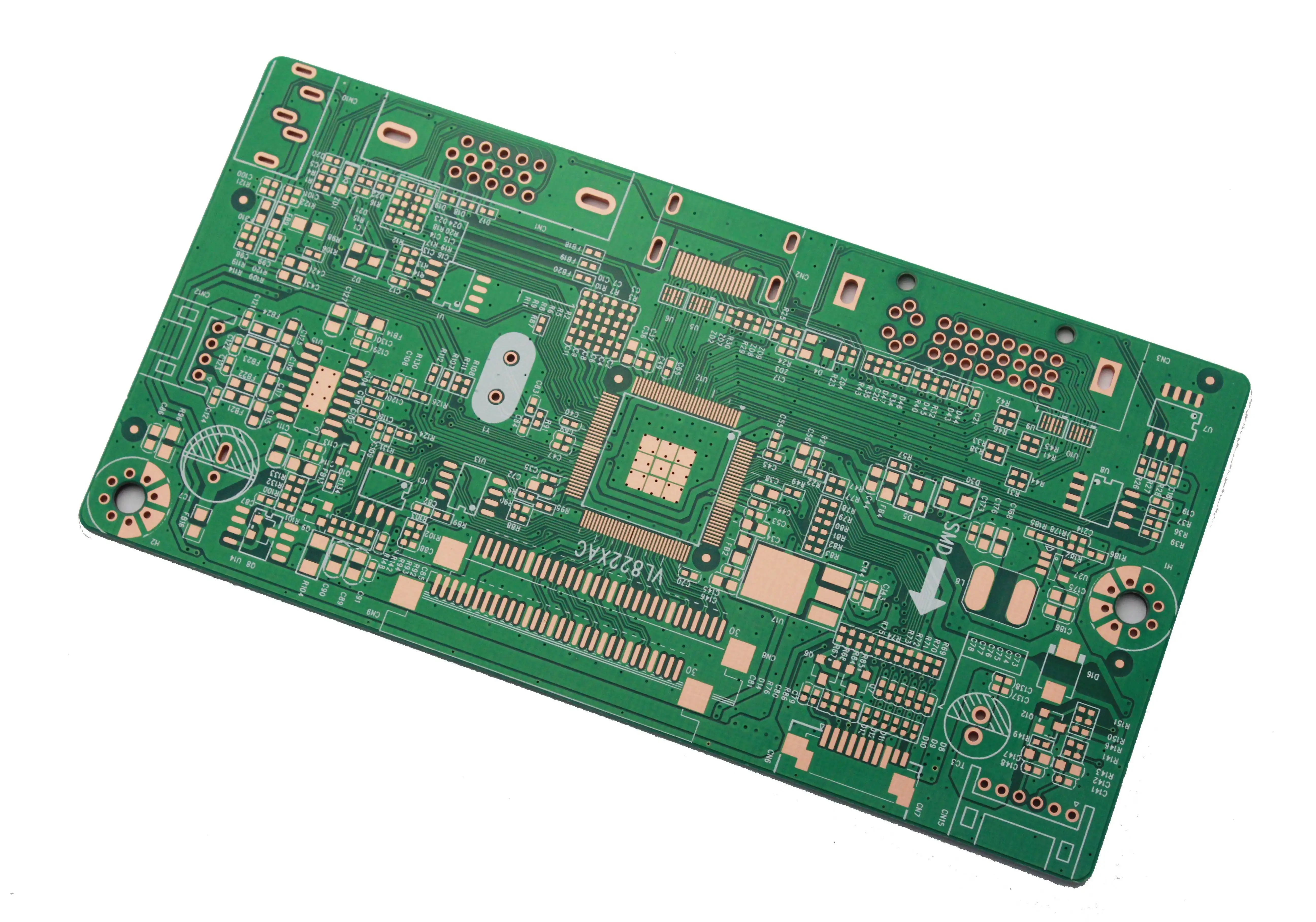
PCB design engineers often want to use automatic wiring when designing PCB. In general, it is no problem to use automatic wiring for purely digital circuit boards (especially when the signal level is low and the circuit density is small). However, when designing analog, mixed signal or high-speed circuit boards, if the automatic routing tool of PCB design software is used, some problems may occur, even serious circuit performance problems may be caused. Figure 1 Top layer of the circuit board designed for the circuit schematic diagram shown in Figure 3 using automatic wiring Figure 2 Top layer of the circuit board designed for the circuit schematic diagram shown in Figure 3 using automatic wiring Figure 3a Circuit schematic diagram of wiring in Figure 1, Figure 2, Figure 4 and Figure 5 Figure 3b Circuit schematic diagram of analog part of wiring in Figure 1, Figure 2, Figure 4 and Figure 5. For example, Figure 1 shows the top layer of a double-sided board designed for automatic wiring. The bottom layer of the double-sided PCB board is shown in Figure 2, and the circuit schematic diagrams of these wiring layers are shown in Figures 3a and 3b.
When designing this mixed signal circuit board, after careful consideration, the devices are manually placed on the board to separate the digital and analog devices. There are several aspects to pay attention to when using this wiring scheme, but the most troublesome is grounding. If the ground wire is laid on the top layer, the components on the top layer are grounded through wiring. The device is also grounded at the bottom layer, and the ground wires at the top layer and bottom layer are connected through the via at the right side of the circuit board. When checking this cabling strategy, it is first found that there are multiple ground loops. In addition, it is also found that the return path of the ground wire at the bottom layer is cut off by the horizontal signal wire. The advantage of this grounding scheme is that the analog devices (12 bit A/D converter MCP3202 and 2.5V reference voltage source MCP4125) are placed on the far right side of the circuit board. This layout ensures that there is no digital ground signal under these analog PCBA chips. The manual wiring of the circuit shown in Fig. 3a and Fig. 3b is shown in Fig. 4 and Fig. 5.

In manual wiring, in order to ensure the correct implementation of the circuit, we need to follow some general design guidelines: try to use the ground plane as the current loop; Separate the analog ground plane from the digital ground plane; If the ground plane is separated by signal wiring, the signal wiring shall be perpendicular to the ground plane to reduce the interference to the ground current circuit; The analog circuit shall be placed as close as possible to the edge of the circuit board, and the digital circuit shall be placed as close as possible to the power connection end, so as to reduce the di/dt effect caused by the digital switch. These two kinds of double-sided boards are laid with ground plane at the bottom layer, which is convenient for PCBAengineers to solve problems, so that they can quickly understand the wiring of the circuit board. The manufacturer's demonstration board and evaluation board usually adopt this cabling strategy. However, it is more common to lay the ground plane on the top of the circuit board to reduce electromagnetic interference.


Just upload Gerber files, BOM files and design files, and the KINGFORD team will provide a complete quotation within 24h.