
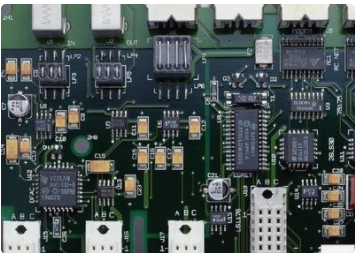
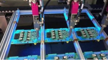
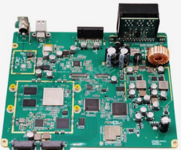
Professional PCB manufacturing and assembly
Building 6, Zone 3, Yuekang Road,Bao'an District, Shenzhen, China
+86-13410863085Mon.-Sat.08:00-20:00

The following describes the difference between electroplating water, sputtering and evaporation in PCB plating surface in PCB factory
PCB electroplating can generally be divided into the following categories:
1. Steam plating: surface adhesion;
2. Sputtering: surface exchange;
3. Water plating: molecular binding
PCB evaporation and PCB sputtering are both used to deposit various metal and non-metallic films on the surface of plastic parts by distillation or sputtering under vacuum conditions. By this way, very thin surface coatings can be obtained, and at the same time, they have the outstanding advantages of fast speed and good adhesion. Vacuum evaporation is a method of heating metal under high vacuum to make it melt, evaporate, and form a metal film on the surface of the sample after cooling. The metal used for evaporation is Al, gold, etc.

What are the differences in conductivity between these different electroplating methods?
General electroplating refers to water plating. Water plating is conductive. What about the adhesion and wear resistance of non-conductive surface with discontinuous coating in vacuum plating? Because electroplating is generally used as the surface (external surface), sputtering is mainly used for the internal surface (EMI prevention, but also for the surface treatment of small keys, such as some keys). In contrast, the film thickness of water electroplating is about 0.01-0.02MM, and the film thickness of vacuum sputtering is about 0.005MM. The abrasion resistance and adhesion of electroplating are relatively good.
Vacuum sputter plating
It mainly uses glow discharge to impact argon (Ar) ions on the target surface, and the atoms of the target are ejected and stacked on the substrate surface to form a film. The properties and uniformity of sputtered film are better than that of evaporated film, but the coating speed is much slower than that of evaporated film. Almost all new sputtering equipment use powerful magnets to spiral electrons to accelerate the ionization of argon around the target, which increases the probability of impact between the target and argon ions and improves the sputtering rate. Generally, metal coatings are mostly DC sputtered, while non-conductive ceramic materials are RF AC sputtered. The basic principle is to use glow discharge to impact argon (Ar) ions on the target surface in vacuum. Cations in the plasma will accelerate towards the negative electrode surface as the sputtered material. This impact will make the target material fly out and deposit on the substrate to form a film. In general, there are several characteristics of thin film coating using the sputtering process:
(1) Metals, alloys or insulators can be made into film materials.
(2) Under the appropriate setting conditions, the film with the same composition can be made from the multiple and complex target materials.
(3) The mixture or compound of target material and gas molecules can be made by adding oxygen or other active gases into the discharge atmosphere.
(4) The input current and sputtering time of the target can be controlled, and high precision film thickness can be easily obtained.
(5) Compared with other processes, it is advantageous to produce large area uniform films.
(6) Sputtered particles are hardly affected by gravity, and the positions of target and substrate can be arranged freely.
(7) The adhesion strength between the PCB substrate and the film is more than 10 times that of the general evaporation film. Because the sputtered particles have high energy, they will continue to diffuse on the film forming surface to obtain a hard and dense film. At the same time, this high energy enables the substrate to obtain a crystalline film at a lower temperature.
(8) At the initial stage of film formation, the nucleation density is high, and extremely thin continuous films below 10nm can be produced.
(9) The target material has a long life and can be produced automatically and continuously for a long time.
(10) The target can be made into various shapes, which can be used for better control and most efficient production with the special design of the machine. The coating thickness of PCB water plating is thicker than that of vacuum plating, and the wear resistance is also better than that of real plating.
To sum up, the differences between the plating processes of circuit boards are as follows:
1. The vacuum plating process is environmentally friendly, and there are hidden dangers in water plating.
2. The vacuum plating process is similar to the baking varnish process, but the water plating process is different.
3. The adhesion of vacuum plating is higher than that of water plating, so UV should be added.


Just upload Gerber files, BOM files and design files, and the KINGFORD team will provide a complete quotation within 24h.