
Professional PCB manufacturing and assembly
Building 6, Zone 3, Yuekang Road,Bao'an District, Shenzhen, China
+86-13410863085Mon.-Sat.08:00-20:00

High precision refers to the use of fine line width/spacing, micro holes, narrow ring width (or no ring width), buried, blind holes and other technologies to achieve high density.
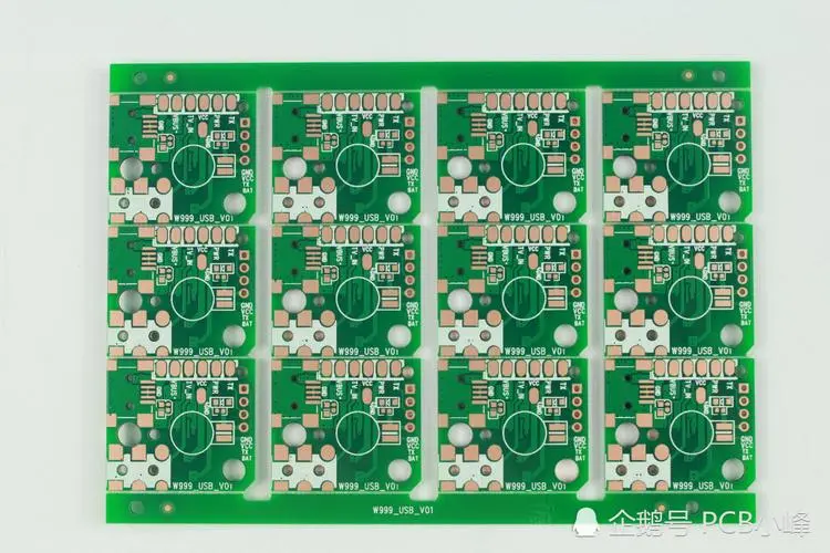
Pcb circuit board
High precision means that the result of "thin, small, narrow and thin" will inevitably lead to high precision requirements. Take the line width as an example:
0.20mm line width, 0.16-0.24mm produced according to the regulations is qualified, and the error is (0.20 ± 0.04) mm; Similarly, the error of 0.10mm line width is (0.1 ± 0.02) mm. Obviously, the accuracy of the latter is doubled. It is not difficult to understand the analogy. Therefore, the requirements for high accuracy will not be discussed separately. But it is a prominent problem in production technology.
Fine wire technology
In the future, the high fine line width/spacing will be from 0.20 mm to 0.13 mm to 0.08 mm to 0.005 mm to meet the requirements of SMT and Multichip Package (MCP). Therefore, the following technologies are required.
① Substrate
Thin or ultra-thin copper foil (<18um) substrate and fine surface treatment technology are adopted.
② Process
The thin dry film and wet film pasting process are adopted. The thin and high-quality dry film can reduce line width distortion and defects. Wet pasting can fill small air gap, increase interface adhesion, and improve wire integrity and accuracy.
③ Electrodeposited photoresist film
Electrodeposited photoresist (ED) was used. Its thickness can be controlled within the range of 5~30/um, which can produce more perfect fine wires. It is especially suitable for narrow ring width, no ring width and full plate electroplating. At present, there are more than ten ED production lines worldwide.
④ Directional light exposure technology
The parallel light exposure technology is adopted. Because the parallel light exposure can overcome the influence of the line width variation caused by the oblique rays of the "point" light source, fine wires with accurate line width size and smooth edges can be obtained. However, parallel exposure equipment is expensive, high investment, and requires working in a high cleanliness environment.
⑤ Automatic optical inspection technology
Automatic optical inspection technology is adopted. This technology has become an essential means of detection in the production of fine wires, and is being rapidly promoted, applied and developed.
Microporous technology
The function hole of printed circuit board used for surface mounting of microporous technology mainly plays the role of electrical interconnection, which makes the application of microporous technology more important. Using conventional drill materials and CNC drilling machines to produce micro holes has many faults and high costs.
Therefore, the high-density PCB mainly focuses on the fine densification of wires and bonding pads. Although great achievements have been made, its potential is limited. To further improve the fine densification (such as wires less than 0.08mm), the cost will rise sharply, so micro holes will be used to improve the fine densification.
In recent years, CNC drilling machine and micro drill technology have made breakthrough progress, so micro hole technology has developed rapidly. This is the main outstanding feature in current PCB production.
In the future, the micro hole forming technology will mainly rely on advanced CNC drilling machines and fine micro heads, while the micro holes formed by laser technology are still inferior to those formed by CNC drilling machines in terms of cost and hole quality.
① CNC drilling machine
At present, CNC drilling machine technology has made new breakthroughs and progress. A new generation of CNC drilling machine characterized by drilling micro holes has been formed.
The efficiency of drilling small holes (less than 0.50 mm) by microporous drilling machine is one time higher than that of conventional CNC drilling machine, with fewer failures and rotating speed of 11~15r/min; It can drill 0.1~0.2mm micropores. It uses a high-quality small drill bit with high cobalt content and can stack three plates (1.6mm/piece) for drilling. When the drill bit is broken, it can automatically stop and report the position, automatically change the drill bit and check the diameter (the tool magazine can accommodate hundreds of pieces), and automatically control the constant distance between the drill tip and the cover plate and the drilling depth, so that blind holes can be drilled without damaging the table. CNC drilling machine table adopts air cushion and magnetic levitation, which can move faster, lighter and more accurately without scratching the table.
Such drilling machines are very popular at present, such as the Mega 4600 of Prurite in Italy, the Excelton 2000 series in the United States, and new generation products from Switzerland and Germany.
② Laser drilling
Conventional CNC drilling machine and drill bit do have many problems in drilling micro holes. The development of micro hole PCB technology has been hindered, so laser etching has been paid attention to, studied and applied.
However, there is a fatal disadvantage, that is, the horn hole is formed and becomes serious with the increase of plate thickness. In addition, the pollution caused by high-temperature ablation (especially multilayer boards), the life and maintenance of light sources, the repeated accuracy of etch holes, and the cost are also problems, so the promotion and application of micro holes in PCB production are limited. However, laser etching is still applied to thin high-density microporous plates, especially in the high-density interconnection (HDI) technology of MCM-L, such as M.C The combination of polyester film etching and metal deposition (sputtering technology) in Ms has been applied in high-density interconnects.
Buried hole formation in high-density interconnection multilayer PCB boards with buried and blind hole structures can also be applied. However, due to the development and technical breakthrough of CNC drilling machine and micro drill, it has been rapidly promoted and applied. Therefore, the application of laser drilling in surface mounted circuit boards cannot form a dominant position. But it still has a place in a certain field.
③ Buried, blind and through hole technology
The combination of buried, blind and through hole technology is also an important way to improve the high-density of printed circuit. Generally, the buried and blind holes are micro holes. In addition to increasing the number of PCB wiring on the board, the buried and blind holes are all "nearest" inter layer interconnections, which greatly reduces the number of vias formed and the setting of isolation panels, thus increasing the number of effective wiring and inter layer interconnections in the board and improving the high-density interconnection.
Therefore, the interconnection density of the multilayer board with buried, blind and through holes is at least three times higher than that of the conventional full through hole board structure under the same size and number of layers. If the printed board with buried, blind and through holes is under the same technical indicators, its size will be greatly reduced or the number of layers will be significantly reduced.
Therefore, in the high-density surface mounted PCB boards, the buried and blind hole technology has been increasingly applied, not only in the surface mounted PCB boards of large computers, communication equipment, etc., but also in the fields of civil and industrial use, and even in some thin boards, such as PCMCIA, Smard, IC card and other thin boards with more than six layers.
The printed circuit board with buried and blind hole structure is generally completed by the "separate board" production method, which means that it can only be completed after many times of PCB pressing, drilling, hole electroplating, etc., so precise positioning is very important


Just upload Gerber files, BOM files and design files, and the KINGFORD team will provide a complete quotation within 24h.