
Professional PCB manufacturing and assembly
Building 6, Zone 3, Yuekang Road,Bao'an District, Shenzhen, China
+86-13410863085Mon.-Sat.08:00-20:00

Precautions for clock design on the circuit board are mainly considered from three aspects.
1. PCB layout
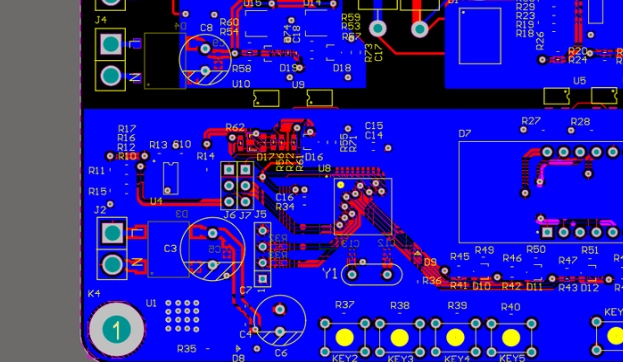
1) Clock crystals and related circuits should be arranged in the center of PCB and have a good stratum, not close to the I/O interface. The clock generation circuit cannot be made into a sub card or sub board, but must be made on a separate clock board or bearing board.
2) In the clock circuit area of PCB, only PCB devices related to the clock circuit shall be laid, and other circuits shall not be laid. No other signal lines shall be laid near or below the crystal. The ground plane shall be used in the clock generating circuit and under the crystal. If other signals pass through the plane, it violates the function of the image plane. If signals pass through the ground plane, there will be a small ground loop and affect the continuity of the ground plane, These ground loops will cause problems at high frequencies.
3) For clock crystals and clock circuits, shielding measures can be taken.
4) If the clock housing is metal, it must be paved with copper under the crystal, and ensure that this part has a good electrical connection with the complete ground plane (through porous grounding).
5) Advantages of laying the ground below the clock crystal: the circuit inside the crystal oscillator will generate RF current. If the crystal is encapsulated in a metal shell, the DC power supply pin is the basis for DC voltage reference and RF current loop reference inside the crystal, and the transient current generated by RF radiation from the shell is released through the ground plane. In a word, the metal shell is a single ended antenna, and sometimes two or more layers of the nearest image layer and ground layer are sufficient as the radiation coupling effect of RF current to the ground. The floor under the crystal is also good for heat dissipation.
6) The clock circuit and the ground laid under the crystal will provide an image plane, which can reduce the common mode current generated on the related crystal and clock circuit, thus reducing the radio frequency radiation. The ground plane also has the absorption effect on the differential mode radio frequency current. This plane must be connected to the complete ground plane through multiple points, and requires multiple vias, which can provide low impedance. To enhance the effect of this ground plane, The clock generation circuit should be close to this ground plane.
7) SMT packaged crystals will have more RF energy radiation than those with metal shells: because most surface mounted crystals are plastic packages, the RF current inside the crystals will radiate into space and be coupled to other devices.
2. Special circumstances and consequences
1) Shared clock routing
For fast rising edge signals and clock signals, radial topology connection is better than serial connection of networks using a single common drive source. Each route shall be wired by taking termination measures according to its characteristic impedance.
2) Clock transmission line requirements and PCB layering
Clock routing principle: arrange a complete image plane layer next to the clock routing layer to reduce the length of the routing and perform impedance control. Incorrect cross layer routing and impedance mismatch will result in:
The use of vias and jumps in wires leads to the incompleteness of the image loop.
The surge voltage generated by the change of the voltage on the signal pin of the PCB device on the image plane with the change of the signal.
If the 3W principle is not considered in wiring, different clock signals will cause crosstalk.
3. PCB wiring
1) The clock line must be on the inner layer of the multilayer PCB board. And must follow the stripline; If you want to walk in the outer layer, you can only use microstrip lines.
2) Walking on the inner layer can ensure the integrity of the image plane. It can provide a low impedance RF transmission path and generate magnetic flux to offset the magnetic flux of their source transmission lines. The closer the source is to the return path, the better degaussing is. Due to enhanced degaussing capability, each complete planar image layer of high-density PCB can provide 6-8dB suppression.
3) Advantages of the clock cloth multilayer PCB board: one or more layers can be specially used for the complete power supply and ground plane, which can be designed into a good decoupling system, reducing the area of the ground loop, reducing differential mode radiation, reducing EMI, reducing the impedance level of the signal and power supply return path, maintaining the consistency of the impedance of the whole route, reducing the crosstalk between adjacent routes, etc.


Just upload Gerber files, BOM files and design files, and the KINGFORD team will provide a complete quotation within 24h.