
Professional PCB manufacturing and assembly
Building 6, Zone 3, Yuekang Road,Bao'an District, Shenzhen, China
+86-13410863085Mon.-Sat.08:00-20:00

What does additive manufacturing mean to circuit board designers, especially in relation to solder resistance. Here are some important factors that I think designers should consider.
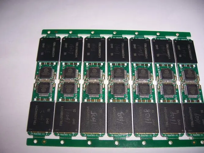
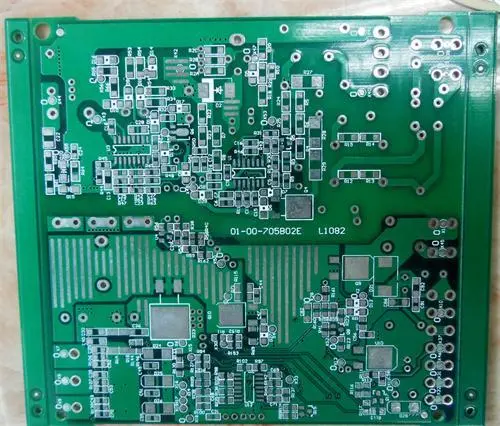
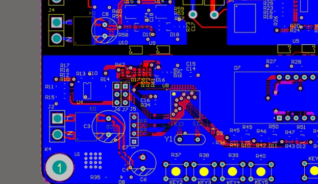
Circuit board design
1. Definition of PCB resistance welding
In essence, the definition provided by any EDA tool is incorrect; CAM vector files specify deviations that assume continuous surfaces. So far, resistance welding technology has been in the form of reduction. SUSS MicroTec has developed a front-end JETxSMFE that can run on CAM workstations to simplify the manufacturing process. The PCB software can interpret all relevant information and correctly control the details of the incoming documents.
2. Advantages of inkjet resistance welding process
One of the advantages of the inkjet resistance welding process is that it can avoid filling any holes or through holes. Some people in the industry may not be able to completely "hide". However, the industry generally believes that the through hole without solder mask improves the reliability of PCB. According to the manufacturing practice, the unmarked drill holes may still be coated with solder mask, which will cause ink on the printing table. This is not a big problem, because the scraper can easily remove excess solder mask ink, and can also replace the workbench or its substrate (if any). However, both solutions can lead to brief downtime. To make a long story short, if you want to make the workshop work smoothly, you must specify all drilling requirements in the design.
3. Rules for welding resistance bridge
The solder mask routing on the laminate separates two nearby copper pads. This figure represents the pad design selection of non solder mask defined (NSMD for short). However, there are several limitations to this choice, resulting in the artificial demand for narrow resistance welding dams. Start with numbers: imagine two PCB pads, 200 µ m apart, nothing special. What is the maximum size of the solder bridge between the two? If LDI process is used, its size comes from the latest constraint of applying the PCB technology. This 200 µ m spacing decreases with the laser beam width plus twice the alignment accuracy (down to 100 µ m). Any more challenging pad distances will also make it more difficult to define the solder bridge rule.
Based on this reasoning, many requirements for building resistance bridges of 50 µ m or less using traditional technologies seem reasonable. So how to deal with inkjet printing? Does it join the last 1 micron challenge? No, on the contrary, it challenges the original design choice and causes debate: PCB solder mask defined (SMD for short) pad or NSMD pad? Neither. On the contrary, it is a pad defined solder mask (PDSM for short). However, this acronym has not been confirmed by the industry, so it cannot be searched by Google. Ink jet printing is a volume driven coating technology, which means it is possible to fill gaps, and even encourages the use of this method.
4. Defined thickness
The controllable thickness means the relationship between the conformability of the coating and the flatness independent of the surface morphology. Which thickness design scheme is more suitable for resistance welding? PCB designers should know exactly the function of solder mask. "Ink jet upgrade" summarizes the basic knowledge: although copper without solder mask will be oxidized, the laminate will not; High voltage copper wiring without solder mask may cause short circuit, while bare laminate will not, so the laminate does not need solder mask. The reason for the current solder barrier coating is that it is convenient (less developer is used) and provides support for any formwork frame. The first problem is no longer a problem, because ink-jet does not use developing chemicals; The second problem is that inkjet is more attractive and can shape grids or arrays, significantly reducing coating materials and providing the same support
Combining the concept of constant coating thickness with PDSM, a new density can be built for the ball grid array (BGA) structure.
5. Design Rule Inspection
Here are a series of considerations, which belong to the scope of design rule inspection, and are finally checked by CAM software. However, the following instructions can avoid misunderstanding by the manufacturer. Designers must understand:
The solder mask has a minimum radius, which largely depends on the inkjet equipment selected.
The minimum feasible gap between solder mask features is less than the minimum feasible print solder mask feature.
The thinner solder mask layer allows smaller feature size, on the contrary, the thicker copper layer or thick solder mask layer will increase the minimum feature size.
The profile of a narrow solder mask is similar to a dome. The traditional rectangular section no longer exists. Instead, it is a contour without edges and cavities, which improves the mechanical and chemical stability.
PCB solder mask structure is layer based. This means that other geometric features can also be added at the top of the solder mask for mechanical support of the element or spot coating limits.
As mentioned earlier, current CAM solutions can handle details such as solder mask thickness, copper thickness, and drilling, but cannot define their correct locations. The most ideal solution should be integrated and integrated in CAM software or design tools, which can define the required solder mask thickness of components at each position. PCB designers will add all information at the component level to prevent tombstone effects.


Just upload Gerber files, BOM files and design files, and the KINGFORD team will provide a complete quotation within 24h.