
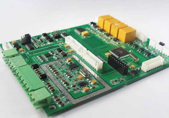
Professional PCB manufacturing and assembly
Building 6, Zone 3, Yuekang Road,Bao'an District, Shenzhen, China
+86-13410863085Mon.-Sat.08:00-20:00

Differential mode current and common mode current
Radiation generation: current causes radiation rather than voltage, static charge generates electrostatic field, constant current generates magnetic field, and time-varying current generates both electric field and magnetic field. Common mode current and differential mode current exist in any circuit. Differential mode signal carries data or useful signals. Common mode signal is the negative effect of differential mode.
Differential mode current: equal in magnitude and opposite in direction (phase). Due to the discontinuous distributed capacitance, inductance and signal line impedance of the pcb wiring, and the unexpected path of the signal return path, the differential mode current will be converted into the common mode c

urrent. The common mode current is not necessarily the same in size and direction (phase).
The external interference of equipment is mainly common mode, and differential mode interference also exists, but the common mode interference intensity is often several orders of magnitude greater than the differential mode intensity. The external interference is mainly common mode interference, which generally does not harm the equipment. However, if the common mode interference is converted into differential mode interference, it will be serious, because the useful signals are differential mode signals.
The magnetic field of differential mode current is mainly concentrated in the loop area formed by differential mode current, while the magnetic lines of force will cancel each other outside the loop area; The magnetic field of common mode current is outside the loop area, and the magnetic field generated by common mode current has the same direction.
Many EMC designs of PCB follow the above theory.
The way to suppress interference on PCB board is to reduce the area of differential mode signal loop.
Reduce high-frequency noise return (filtering, isolation and matching).
Reduce common mode voltage (grounding design).
Summary of PCB design principles
Principle 1: The PCB clock frequency exceeds 5MHZ or the signal rise time is less than 5ns, which generally requires the use of multilayer board design.
Cause: The area of the signal loop can be well controlled by using the multilayer board design.
Principle 2: For the key wiring layer (the layer where clock line, bus, interface signal line, RF line, reset signal line, chip selection signal line and various control signal lines are located), it should be adjacent to the complete ground plane, preferably between the two ground planes.
Reason: The key signal lines are generally strong radiation or extremely sensitive signal lines. Wiring close to the ground plane can reduce the area of the signal circuit, reduce its radiation intensity or improve the anti-interference ability.
Principle 3: For single-layer boards, both sides of key signal lines should be wrapped;
Reason: The two sides of the key signal are grounded, which can reduce the area of the signal loop on the one hand, and prevent the crosstalk between the signal line and other signal lines on the other hand.
Principle 4: For the double-layer board, the projection plane of the key signal line has a large area of floor covering, or the same as the single panel is punched.
Cause: The key signal is the same as that of the multilayer board near the ground plane
Principle 5: In a multilayer board, the power plane should be reduced by 5H-20H relative to its adjacent ground plane (H is the distance between the power and ground plane).
Cause: Shrinking the power plane relative to its return ground plane can effectively suppress the edge radiation problem.
Principle 6: The projection plane of the wiring layer should be within the area of its return plane layer.
Cause: If the wiring layer is not within the projection area of the return plane layer, it will cause edge radiation problems, and increase the area of the signal loop, which will lead to increased differential mode radiation.
Principle 7: In multilayer boards, there should be no signal lines larger than 50MHZ at the TOP and BOTTOM layers of boards,
Reason: It is better to walk the high-frequency signal between two plane layers to inhibit its radiation to space.
Principle 8: For boards with a board level operating frequency greater than 50MHz, if the second layer and the penultimate layer are wiring layers, the TOP and BOOTTOM layers should be paved with grounding copper foil.
Reason: It is better to walk the high-frequency signal between two plane layers to inhibit its radiation to space.
Principle 9: In multilayer boards, the main working power plane (the most widely used power plane) of a single board should be close to its ground plane.
Cause: The power plane adjacent to the ground plane can effectively reduce the loop area of the power circuit.
Principle 10: In a single-layer board, there must be a ground wire adjacent to and parallel to the power line.
Cause: Reduce the area of power current loop.
Principle 11: In the double-layer board, there must be a ground wire adjacent to and parallel to the power line.
Cause: reduce the area of power current loop
Principle 12: In the layered design, try to avoid the adjacent settings of the wiring layer. If the adjacent wiring layers cannot be avoided, the layer spacing between the two wiring layers should be appropriately increased, and the layer spacing between the wiring layers and their signal circuits should be reduced.
Cause: Parallel signal routing on adjacent wiring layers will cause signal crosstalk.
Principle 13: Adjacent plane layers shall avoid overlapping of their projection planes.
Cause: When the projection overlaps, the coupling capacitance between layers will cause the noise between layers to be coupled.
Principle 14: During PCB layout design, the design principle of linear placement along the signal flow direction shall be fully followed, and loop back and forth shall be avoided as far as possible.
Cause: Avoid direct coupling of signals, which affects signal quality.
Principle 15: When multiple module circuits are placed on the same PCB, digital circuits and analog circuits, high-speed and low-speed circuits shall be arranged separately.
Cause: Avoid mutual interference between digital circuits, analog circuits, high-speed circuits and low-speed circuits.
Principle 16: When there are high, medium and low speed circuits on the circuit board at the same time, the high and medium speed circuits should be kept away from the interface.
Cause: Prevent high-frequency circuit noise from radiating outward through the interface.
Principle 17: Energy storage and high-frequency filter capacitors shall be placed near unit circuits or devices with large current changes (such as input and output terminals of power modules, fans and relays).
Cause: The existence of energy storage capacitor can reduce the loop area of high current loop.
Principle 18: The filter circuit of the power input port of the circuit board shall be placed close to the interface,
Cause: Avoid the lines that have been filtered from being coupled again.
Principle 19: On the PCB board, the filtering, protection and isolation devices of the interface circuit should be placed close to the interface.
Cause: It can effectively achieve the effects of protection, filtering and isolation.
Principle 20: If there are both filtering and protection circuits at the interface, the principle of protection before filtering should be followed.
Cause: The protection circuit is used for external overvoltage and overcurrent suppression. If the protection circuit is placed behind the filter circuit, the filter circuit will be damaged by overvoltage and overcurrent.
Principle 21: The layout shall ensure that the input and output lines of filter circuit (filter), isolation and protection circuit are not coupled with each other.
Cause: When the input and output wiring of the above circuits are coupled with each other, the filtering, isolation or protection effects will be weakened.
Principle 22: If the interface on the board is designed to be "clean", the filter and isolation devices should be placed on the isolation belt between the "clean" and the working place.
Cause: Avoid mutual coupling of filter or isolation devices through the plane layer to weaken the effect.
Principle 23: Do not place any other devices except filter and protective devices on the "clean ground".
Reason: "Clean" design aims to ensure minimum interface radiation, and "clean" is easily coupled by external interference, so there should be no other irrelevant circuits and devices on the "clean".
Principle 24: Crystal, crystal oscillator, relay, switching power supply and other strong radiation devices shall be at least 1000 mil away from the interface connector of the single board.
Cause: The interference will radiate outward directly or couple the current on the outgoing cable to radiate outward.
Principle 25: Sensitive circuits or devices (such as reset circuits, WATCHDOG circuits, etc.) shall be at least 1000 mils away from the edges of boards, especially the edges of board interfaces.
Cause: Places like the board interface are most susceptible to external interference (such as static electricity) coupling, while sensitive circuits such as reset circuit and watchdog circuit are very likely to cause the system
Misoperation.
Principle 26: All filter capacitors used for IC filtering should be placed as close as possible to the power supply pin of the chip.
Cause: The closer the capacitor is to the pin, the smaller the area of the high-frequency circuit, and thus the smaller the radiation.
Principle 27: The matching resistor in series at the starting end shall be placed close to its signal output end.
Cause: The design purpose of the series matching resistance at the beginning is to make the sum of the output impedance of the chip output end and the impedance of the series resistance equal to the characteristic impedance of the wiring. The matching resistance is placed at the end, which cannot meet the above equation.
Principle 28: PCB wiring shall not have right angle or acute angle wiring.
Cause: The right angle wiring leads to discontinuous impedance, leading to signal transmission, resulting in ringing or overshoot, forming strong EMI radiation.
Principle 29: Avoid the layer setting of adjacent wiring layers as much as possible. If it cannot be avoided, try to make the routing in the two wiring layers perpendicular to each other or the parallel routing length less than 1000 mils.
Cause: reduce crosstalk between parallel lines.
Principle 30: If the board has an internal signal routing layer, the clock and other key signal lines are routed in the internal layer (priority is given to the routing layer).
Cause: The key signals can be shielded by laying them on the internal wiring layer.
Principle 31: It is recommended to wrap the ground wire on both sides of the clock wire, and the grounding via should be drilled every 3000mil.
Cause: ensure that the potential of each point on the grounding wire is equal.
Principle 32: Clock, bus, RF cable and other key signal wiring and other parallel wiring on the same layer shall meet the 3W principle.
Cause: Avoid crosstalk between signals.
Principle 33: The bonding pads of surface mounted fuses, magnetic beads, inductors and tantalum capacitors used for power supply with current ≥ 1A shall be connected to the plane layer through at least two vias.
Cause: reduce the equivalent impedance of vias.
Principle 34: The differential signal lines shall be laid in the same layer, of equal length and in parallel, with the same impedance and no other lines between the differential lines.
Reason: ensure the common mode impedance of differential line pair is equal, and improve its anti-interference capability.
Principle 35: The key signal routing must not cross the partition area (including the reference plane gap caused by vias and pads).
Cause: Wiring across the partition will lead to an increase in the area of the signal loop.
Principle 36: When it is unavoidable for the signal line to split the ground across its return plane, it is recommended to use bridge capacitance near the signal cross split, and the capacitance value is 1nF.
Cause: When the signal is split across, the circuit area is often increased. The bridge grounding method is used to set the signal circuit for it manually.
Principle 37: No other irrelevant signals shall be routed below the filter (filter circuit) on the board.
Cause: Distributed capacitance will weaken the filtering effect of the filter.
Principle 38: The input and output signal lines of the filter (filter circuit) shall not be parallel or crossed.
Cause: Avoid direct noise coupling before and after filtering.
Principle 39: The distance between the key signal line and the edge of the reference plane is ≥ 3H (H is the height of the line from the reference plane).
Cause: inhibit the edge radiation effect.
Principle 40: For the grounding element of metal shell, the top layer of its projection area shall be paved with grounding copper sheet.
Cause: The distributed capacitance between the metal shell and the grounding copper sheet is used to restrain its external radiation and improve its immunity.
Principle 41: In single-layer board or double-layer board, attention should be paid to the "loop area minimization" design when wiring.
Cause: The smaller the loop area is, the smaller the external radiation of the loop is, and the stronger the anti-interference ability is.


Just upload Gerber files, BOM files and design files, and the KINGFORD team will provide a complete quotation within 24h.